| Home | About Us | Contribute | Bookstore | Advertising | Subscribe for Free NOW! |
| News Archive | Features | Events | Recruitment | Directory |
News
3 September 2010
Taiwan researchers show how patterned LED lift-off boosts photoluminescence
Researchers at Taiwan’s National Chung Hsing University (NCHU) have developed a chemical technique to ‘lift-off’ indium gallium nitride (InGaN) light-emitting diodes from the sapphire substrate used to grow the nitride semiconductor [Chia-Feng Lin et al, Appl. Phys. Express, vol3, p092101, 2010]. The resulting LEDs had a photoluminescence spectrum that was enhanced 2.2x over a standard device. The lift-off technique resulted in a GaN surface patterned with V-shape grooves.
A number of techniques have been developed in the past few years to increase light extraction from nitride LEDs. Patterning in strategic locations is widely used to reduce the reflection of light at interfaces back into devices. Also, removal of some layers, such as the sapphire substrate, can increase light output power. Laser lift-off is one technique used to do this. Other groups have experimented with various chemical lift-off (CLO) methods using sacrificial layers of materials such as chromium nitride and zinc oxide.
The NCHU group has developed a CLO using aluminum nitride (AlN) sacrificial layers. The 2-inch sapphire substrate was patterned using a 200nm silicon dioxide mask layer with 1μm stripes spaced 2μm apart. The sapphire was etched using a hot of sulfuric/phosphoric acid solution and the SiO2 mask was then removed. This resulted in a series of triangle-shaped grooves in the sapphire substrate.
The LED structures were then grown on the patterned substrates using metal-organic chemical vapor deposition (MOCVD). The main sources were trimethyl-Ga, -In, -Al, and ammonia (NH3). For the silicon (n-type) and magnesium (p-type) doping, silane (SiH4) and bis(cyclopentadienyl)magnesium (Cp2Mg) were used.
Aluminum nitride was used as a 30nm sacrificial layer for the chemical lift-off process (Figure 1). The LED structure consisted of 5.5μm n-GaN, a 10-period multi-quantum well (3nm InGaN well, 7nm GaN barrier) light-emitting active layer and 0.2μm p-GaN.
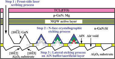
Figure 1 (above): Schematic diagram of the LED structure for the chemical lift-off process.
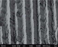 Figure 2 (right): Scanning electron micrograph showing V-shaped grooves in lift-off GaN surface.
The 400x136μm LED mesas were covered with indium tin oxide (ITO) transparent conducting material. The mesas were produced using a laser scribe, then a hot 80°C potassium hydroxide solution was used to create grooves in the nitrogen face of the n-GaN layer. The etch stop consisted of the stable {10-1-1} face of the GaN material. The final part of the chemical lift-off process was to laterally etch the AlN sacrificial layer. After the 15-minute wet etch, the individual LED chips were removed using adhesive tape.
The resulting LEDs were inspected using optical and electron micrography. Photoluminescence experiments with a 405nm excitation laser revealed a peak at 440.7nm (blue). LEDs created using the same process, but without removing the sapphire, had a peak at the slightly longer wavelength of 445.8nm. The peak for the CLO-LED was enhanced 2.2x over the standard device. The researchers suggest that the slight difference in wavelength between the devices was due to release of the compressive strain at the sapphire–nitride interface.
The electroluminescence (EL) peak was 455.9nm at 1mA and 453.0nm at 5mA, the blueshift being attributed to ‘band filling’ as the electron levels fill up at higher currents, increasing the effective energy separation between the electron and hole levels.
The relatively high forward voltage of 4.14V at 20mA was attributed to a non-optimized ohmic contact to the n-GaN lift-off layer. The EL measurements were carried out with the ITO layer connecting with a copper substrate, and the electrical contacts were made with probes.
![]() Search: InGaN LEDs Lift-off Sapphire substrate
Search: InGaN LEDs Lift-off Sapphire substrate
Visit: http://apex.ipap.jp/link?APEX/3/092101
Visit: www.nchu.edu.tw
For more on LEDs: Latest issue of Semiconductor Today
The author Mike Cooke is a freelance technology journalist who has worked in the semiconductor and advanced technology sectors since 1997.
![]() ©2010 Juno Publishing and Media Solutions Ltd. All rights reserved. Semiconductor Today and the editorial material contained within it and related media is the copyright of Juno Publishing and Media Solutions Ltd. Reproduction in whole or part without permission from Juno Publishing and Media Solutions Ltd is forbidden. In most cases, permission will be granted, if the author, magazine and publisher are acknowledged.
©2010 Juno Publishing and Media Solutions Ltd. All rights reserved. Semiconductor Today and the editorial material contained within it and related media is the copyright of Juno Publishing and Media Solutions Ltd. Reproduction in whole or part without permission from Juno Publishing and Media Solutions Ltd is forbidden. In most cases, permission will be granted, if the author, magazine and publisher are acknowledged.
Disclaimer: Material published within Semiconductor Today and related media does not necessarily reflect the views of the publisher or staff. Juno Publishing and Media Solutions Ltd and its staff accept no responsibility for opinions expressed, editorial errors and damage/injury to property or persons as a result of material published.
Semiconductor Today, Juno Publishing and Media Solutions Ltd, Suite no. 133, 20 Winchcombe Street, Cheltenham, GL52 2LY, UK
Web site by No Name No Slogan ![]()