| Home | About Us | Contribute | Bookstore | Advertising | Subscribe for Free NOW! |
| News Archive | Features | Events | Recruitment | Directory |
News
21 September 2010
UCSB achieves semi-polar light extraction comparable to conventional LEDs
Researchers at University of California Santa Barbara (UCSB) have improved the extraction efficiency of light-emitting diodes (LEDs) grown on semi-polar nitride substrates to the level of conventional c-plane devices [Yuji Zhao et al, Appl. Phys. Express, vol3, p102101, 2010]. At a drive current of 20mA, the devices emitted 31.1mW, with an external quantum efficiency (EQE) of 54.7%.
Non-polar and semi-polar nitride materials are expected to produce improved light-emitting devices because of reduced spontaneous and strain-dependent (piezoelectric) polarization fields. Such polarization fields tend to pull electrons and holes apart in the light-emitting active region, reducing the chances of recombination occurring as photons.
Semi-polar material has been used to create in the laboratory some of the longest-wavelength-emitting nitride LEDs (up to ~531nm, green), where conventional c-plane material fails to produce working devices. However, up to now the efficiency of sem/non-polar devices emitting blue or violet light has not reached that of traditional c-plane devices.
Often, such devices are limited by the extraction efficiency. The critical angle for the escape cone from a smooth gallium nitride-air interface is low (23°) due to the large difference in refractive indices of the respective substances (2.5/1). Surface texturing/roughening of the gallium nitride (GaN) or sapphire escape surface has been used widely to improve extraction efficiency. These techniques have been widely applied to c-plane devices, but not to the presently non-commercial laboratory demonstrations of semi/non-polar devices.
In their latest work, UCSB (with Kenji Fujito of Mitsubishi Chemical Corp) has produced semi-polar LEDs with conical surface roughening structures that can increase light extraction efficiency and output power by up to 2.8x. The scientists comment: “Semi-polar GaN LED technology is now comparable to commercial c-plane blue LED technology, not only in terms of internal material properties but also in terms of chip processing techniques.”
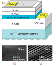 Figure 1: (a) Schematic of semi-polar (10-1-1) LED device with backside roughening structures. SEM images of the backside of the GaN substrate (b) before and (c) after roughening, from a 10° tilted angle.
Mitsubishi Chemical supplied the free-standing (10-1-1) GaN substrates. Metal-organic chemical vapor deposition (MOCVD) was used to deposit the epitaxial nitride semiconductor structures (Figure 1). The n-type (silicon-doped) GaN contact layer was 1μm thick. A 16nm p-type (magnesium-doped) Al0.15Ga0.85N was deposited after the three-period InGaN/GaN quantum well to block electrons from entering the p-contact region. Such electron overshoot reduces LED efficiency by allowing recombination to occur via routes other than through the desired photon emission. The p-GaN contact layer was 60nm thick. Indium tin oxide (ITO) was evaporated onto the p-GaN.
LEDs were fabricated by etching 490x292μm and 2000x500μm mesas using a chlorine-based inductively coupled plasma (ICP). The metal contacts were formed using evaporation and lift-off.
The roughening into cone structures was achieved by using lithography and ICP etching. The plasma consisted of a boron trichloride and chlorine mix designed to produce sidewalls with 58° slopes. The roughening was optimized by varying the density (5.8x10⁵/cm2, 9.0x10⁵/cm2 and 1.6x10⁶/cm2, with top diameter 3μm) and top diameters (2μm, 3μm and 4μm, with density 1.6x10⁶/cm2) of the cones. The output power increased with density, but the improvement with feature diameter saturated for 4μm diameter cones.
Comparisons between experiment and ray-tracing simulations suggest that increasing the feature density to 2.0x10⁶/cm2 could prove beneficial. Although the paper does not give spectral information on the experimental LEDs, the simulations were based on a Gaussian spectrum with a peak emission of 455nm (blue) and full-width at half-maximum (FWHM) of 15nm.
Although the trends were similar between experiment and simulation, the absolute values were discrepant (experimental enhancement over smooth surface was greater). The researchers suggest that this was due to c-plane material parameters without including polarization and birefringence effects of the (10-1-1) material actually used.
On the basis of the optimization experiments, the researcher created 500μm x 2000μm LEDs with 4μm diameter cones at a density of 1.6x10⁶/cm2. The chips were diced and assembled into vertical stand transparent packages.
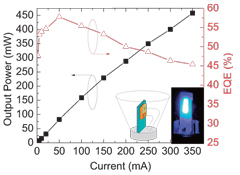 Figure 2: Light output power vs current and EQE vs current for packaged (10-1-1) LED with backside roughening under pulsed conditions. Insets: schematic graph (left) and optical micrograph (right) of working blue LED in transparent packaging.
Electroluminescence measurements were carried out at room temperature using a pulsed current source (1% duty cycle) to avoid self-heating effects. The light output power (Figure 2) measured in an integrating sphere was 31.1mW at 20mA (external quantum efficiency of 54.7%). By 354mA, the external quantum efficiency has dropped to 45.4% (output power 458mW).
The researchers comment: “All of the above numbers are the highest ever reported for semi-polar or non-polar LEDs, and are comparable to those of the best state-of-the-art c-plane LEDs. Moreover, the roughened devices demonstrated a better performance by having a sixfold increase of the output power after packaging, compared with a fourfold increase in the case of conventional devices mainly due to the dramatic enhancement of photon extraction from the backside of the substrate.”
On the basis of their work, the UCSB team concludes: “Our work shows that semi-polar devices are now capable of competing with c-plane devices in the visible spectrum and, with future optimization, higher performance can be expected from these devices.”
![]() Search: LEDs Semi-polar nitride substrates AlGaN InGaN/GaN MQWs MOCVD
Search: LEDs Semi-polar nitride substrates AlGaN InGaN/GaN MQWs MOCVD
Visit: http://apex.ipap.jp
For more on LEDs: Latest issue of Semiconductor Today
The author Mike Cooke is a freelance technology journalist who has worked in the semiconductor and advanced technology sectors since 1997.
![]() ©2010 Juno Publishing and Media Solutions Ltd. All rights reserved. Semiconductor Today and the editorial material contained within it and related media is the copyright of Juno Publishing and Media Solutions Ltd. Reproduction in whole or part without permission from Juno Publishing and Media Solutions Ltd is forbidden. In most cases, permission will be granted, if the author, magazine and publisher are acknowledged.
©2010 Juno Publishing and Media Solutions Ltd. All rights reserved. Semiconductor Today and the editorial material contained within it and related media is the copyright of Juno Publishing and Media Solutions Ltd. Reproduction in whole or part without permission from Juno Publishing and Media Solutions Ltd is forbidden. In most cases, permission will be granted, if the author, magazine and publisher are acknowledged.
Disclaimer: Material published within Semiconductor Today and related media does not necessarily reflect the views of the publisher or staff. Juno Publishing and Media Solutions Ltd and its staff accept no responsibility for opinions expressed, editorial errors and damage/injury to property or persons as a result of material published.
Semiconductor Today, Juno Publishing and Media Solutions Ltd, Suite no. 133, 20 Winchcombe Street, Cheltenham, GL52 2LY, UK
Web site by No Name No Slogan ![]()