- News
15 April 2011
Te doping opens up tunnel junction for GaInP/GaAs solar cells
Korea’s Advanced Nano Fab Center and Hanbat National University have been investigating the use of tellurium (Te) doping in tunnel junctions for tandem solar cells that use gallium indium phosphide and arsenide (GaInP/GaAs) structures [Ho Kwan Kang et al, Semicond. Sci. Technol., vol26, p075009, 2011]. Efficiencies of up to 28% were achieved in tandem solar cells grown on p-GaAs substrates with Te-doped junctions. By comparison, a Si-doped comparison device achieved only 11% efficiency
Tellurium provides n-type carriers in GaAs crystal structures. More usually silicon (Si) doping is used for this. One advantage of using Te is lower diffusion, allowing more abrupt structures to be achieved. Also, higher carrier concentrations can be achieved – up to 2x10¹⁹/cm3) – compared with the 5x10¹⁸/cm3 limit of silicon; this limit exists because, at higher Si doping levels, significant self-compensation sets in.
The results from devices grown on p-GaAs substrates are encouraging for proposed triple-junction formats combining the GaInP/GaAs tandem cell with germanium PV devices (GaInP/GaAs/Ge). The process would start with p-Ge substrates, followed by in-situ diffusion of n-type dopant in an epitaxial deposition chamber to form an n–p Ge junction. Then further layers would be applied to create the III-V cells.
The Korean team concludes: “Our work, thus, suggests that the GaAs tunnel junction with Te doping can be utilized to improve the device performance of GaAs-based multi-junction solar cells, although further research work on heavily Te-doped GaAs layers is required to optimize the carrier concentration and crystalline quality”.
The research started with optimization of the Te-doping in GaAs by varying the growth temperature and precursor flow rates. Metal-organic chemical vapor deposition (MOCVD) was used to grow epitaxial structures on GaAs wafers that were miscut 2° in the <111> plane. Such miscutting can lead to better crystal quality in grown epilayers. Trimethyl-gallium (TMGa) and arsine (AsH3) were the precursors for the epitaxial GaAs with hydrogen used as carrier gas. The tellurium doping was supplied by diethyl-tellurium (DETe).
Tunnel junction structures (Figure 1) with Te- and Si-doping were compared in performance. The p-side of the junction was provided through carbon-doping; the other n- and p-type layers were provided by Si- and zinc-doping, respectively. The tunnel junctions were grown at 550°C, minimizing dopant diffusion and segregation effects. Other layers were grown at 680°C.
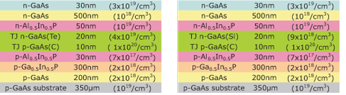
Figure 1: Schematic structures of the tunnel junction diodes: (a) Te/C and (b) Si/C junction.
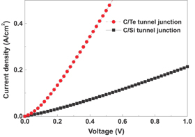 The Te-doping in the tunnel junction provided much higher current densities (Figure 2) for a given voltage. The tunnel junction diode structures were used in GaInP/GaAs tandem solar cells grown on n- and p-GaAs substrates. Low-resistance contact metallization schemes were used: AuGe/Ni/Au for the n-side and Ti/Pt/Au for the p-side. A double-layer anti-reflection coating of SiO2 (600nm)/SiNx(500nm) was also applied to minimize optical losses.
Figure 2: Current–voltage (I–V) curves for the tunnel junction diodes.
The extracted device parameters were determined under air-mass 1.5 global (AM1.5G) solar illumination (Table 1). Te-doped tunnel junctions showed poor performance (7% efficiency, compared with 26% for Si-doped junction) on n-type GaAs substrates with cross-sectional transmission electron microscopy (TEM) investigation showing non-uniform Te-doped layers attributed ‘probably’ to the formation of micro-precipitates of gallium telluride (Ga2Te3). The researchers thus recommend a lower level of Te-doping in this case, giving lower resulting carrier densities.
Solar cells with the GaAs tunnel junction |
||||||||||||
n-tunnel (/cm3) |
p-tunnel (/cm3) |
Substrate |
JSC (mA/cm2) |
VOC (V) |
FF (%) |
Efficiency (%) |
||||||
Si: |
9x10¹⁸ |
C: |
1x10²⁰ |
n-type |
12.39 |
(±0.02) |
2.40 |
(±0.02) |
83.76 |
(±0.41) |
25.53 |
(±0.04) |
Te: |
4x10¹⁹ |
C: |
1x10²⁰ |
n-type |
8.88 |
(±0.04) |
2.15 |
(±0.02) |
35.81 |
(±0.23) |
7.17 |
(±0.03) |
Te: |
1x10¹⁹ |
C: |
1x10²⁰ |
p-type |
14.13 |
(±0.08) |
2.34 |
(±0.01) |
85.08 |
(±0.51) |
28.03 |
(±0.02) |
Si: |
9x10¹⁸ |
C: |
1x10²⁰ |
p-type |
13.12 |
(±0.05) |
1.47 |
(±0.02) |
36.81 |
(±0.18) |
10.51 |
(±0.05) |
Table 1: Summary of measured solar cell performance.
By contrast, on p-GaAs wafers the Te-doped tunnel junction resulted in much better performance compared with Si-doping (28% efficiency vs 11%). The researchers believe that the Si-doped device could have suffered significant out-diffusion of Si into other layers, “especially into the C-doped GaAs layer”. The result of such diffusion would be increased tunneling resistance, degrading solar cell performance. “However, the exact mechanism is under investigation,” the researchers say.
GaInP/GaAs solar cells p-GaAs substrates p-Ge substrates
The author Mike Cooke is a freelance technology journalist who has worked in the semiconductor and advanced technology sectors since 1997.
Join Semiconductor Today's LinkedIn networking and discussion group