- News
19 August 2011
First Chinese Ka-band nitride semiconductor MMIC
Chinese Academy of Sciences (CAS) researchers have extended their work on gallium nitride (GaN) high-electron-mobility capability in the Ka-band (26.5–40GHz) to monolithic microwave integrated circuits [Wang Dongfang et al, J. Semicond., vol32, p085011, 2011]. The researchers from CAS’ Institute of Microelectronics say: “This is, to the best of our knowledge, the first demonstration of domestic [i.e. to China] Ka-band GaN amplifier MMICs.”
The Ka band is used in satellite communications (telecoms and data links, e.g. in Kepler telescope), military high-resolution close-range targeting radar, vehicle speed detection, etc. Chinese MMICs have previously been focused on the C (4–8GHz) and X (8–12GHz) bands.
MMICs integrate microwave transistors, impedance matching and bias elements on one wafer. The researchers used an aluminum gallium nitride (AlGaN) high-electron-mobility transistor (HEMT) with 0.25μm gate length and 2μm x 75μm width. In previous work, the saturated drain current for this device reached 1030mA/mm, and in the Ka-band the maximum stable gain (MSG) was 10.5–11.5dB.
The researchers used a coplanar waveguide (CPW) design (Figure 1) for the MMIC rather than micro-strips, since this made it easier to create the circuit, with fabrication requiring fewer process steps. However, the initial design process is more difficult with CPW circuits. In addition, CPW designs can have a lower thermal resistance, which is important for reducing the operating temperature of devices.
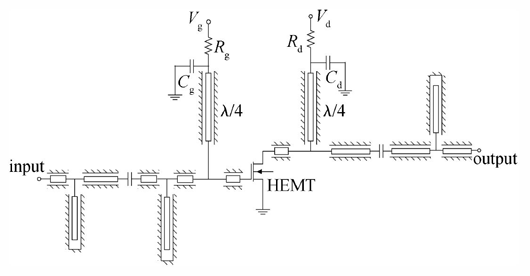
Figure 1: CPW amplifier circuit diagram.
The researchers were unable to use power-matched impedances, since they have been unable to obtain optimal load and source values due to restrictions on measurement capabilities in the Ka-band. Instead the CPW setup was designed to maintain the S-parameter matrix of the HEMT in a suitable state with a drain voltage of 30V and a gate potential of –1.5V.
The flip-chip MMIC also had thermal bumps at the ground-plate for heat removal. The use of flip-chip technology for high-power amplifiers has been estimated to give cost savings of up to 40%.
The CPW transmission lines were designed with 50Ω impedance with a 46μm-wide center conductor and a 15μm-wide ground plate. The target frequency was 32GHz. The quarter-wavelength lengths of transmission line used to feed in the bias potentials were 1.2mm long.
The circuit also needing stabilizing, since just using the transistor with a bias circuit was predicted to be unstable in the range 8–33GHz. This was achieved by adding decoupling capacitors and a stabilizing resistor for both gate and drain, rather than just the gate. Although adding resistance at the drain can reduce power efficiency, the researchers estimate that, under the given bias condition, the power consumed is less than 11mW.
Series and shunt CPW transmission lines were then added to conjugate match the source and drain impedances simulated for the transistor, bias and stabilizing elements. Electromagnetic simulation of the MMIC performance predicted a maximum gain of 8.1dB at 31.5GHz, which is lower than the 9.1dB at 32GHz for the schematic circuit simulation. The difference is attributed to losses in the passive components.
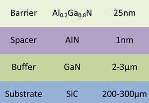 The MMIC was constructed at the CAS’ Institute of Microelectronics on an epitaxial wafer (Figure 2) provided by the CAS’ Institute of Semiconductors. The sheet resistance of this material was 370Ω/square. The processing steps were similar to those used for creating standalone HEMTs: photolithography, etch, titanium-aluminum-nickel-gold ohmic contact metal evaporation, rapid thermal anneal, silicon nitride passivation, electron-beam lithography, dry etch, and T-shaped gate formation. Further processing involved CPW metallization, passivation and electroplating.
Figure 2: Structure of the GaN epitaxial wafer.
The final device (Figure 3) contained the designed MMIC, along with two test HEMTs and two test capacitors for verification/characterization of the discrete device performance. The whole chip measured 2.26mm x 2.36mm.
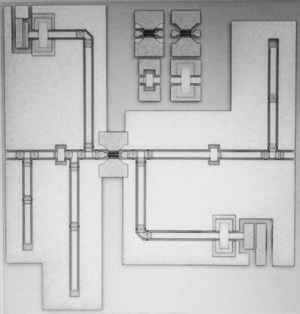 Figure 3: Photo of the Ka-band GaN amplifier MMIC.
The researchers found that the gain and return-loss characteristics of the actual device were better at a source–drain bias (Vds) of 10V, rather than the 30V of the design. Also, there was a shift in the optimum operation frequency, based on S-parameters, from the design’s 32GHz to the range 26–27.5GHz. The peak gain at 26.5GHz was 6.38dB, about 1.7dB lower than that of the design.
The researchers give a number of possible reasons for the discrepancy between the device’s actual and expected performance such as: the structure of the HEMT being different from the group’s previous device on which the design was based (e.g. a 0.2μm larger gate head leading to parasitic capacitance); the epitaxial structure was also somewhat different due to immaturity of the nitride semiconductor growth process (accuracy and stability need to be improved); losses due to metal–SiN insulator–metal capacitances; and finally the simulation software that was used is known to be inaccurate in the Ka-band.
Characterization of the test HEMT showed the cut-off frequency (fT) to be only slightly lower than expected, but the maximum oscillation frequency (fmax) decreased from 120GHz to 91GHz. Also, the maximum stable gain was some 2dB down on the expected performance, with the degradation attributed to the larger gate head size.
Using a Vds of 10V, a continuous-wave 26.5GHz signal showed linear gain of 6.3dB, maximum output power of 22dBm (158mW), and peak power-added efficiency (PAE) of 9.5%. The ‘ultra-low’ PAE is blamed on the lower operating voltage of 10V. This clearly needs to be improved, since a US Army Research Lab team reported in 2006 a peak PAE of 23% and a maximum output power of 4W for a nitride semiconductor MMIC operating at 35GHz.
The new results allowed the researchers to overcome their previous measurement limitations and estimate the maximum output power density in the Ka-band for their HEMTs: 158mW/150μm at 10V and therefore more than 3W/mm at 30V is expected.
The researchers comment: “For future Ka-band GaN MMIC fabrication, it is necessary to improve the consistency of the GaN epitaxial wafer, the stability of the process and the accuracy of the layout simulation.”
The author Mike Cooke is a freelance technology journalist who has worked in the semiconductor and advanced technology sectors since 1997.