- News
5 August 2011
Metal-nitride semiconductor avalanche for UV detection
Researchers in China have reported the first demonstration of a gallium nitride (GaN)-based planar metal-semiconductor-metal avalanche photodiode (APD) sensitive to ultraviolet light [F. Xie et al, IEEE Electron Device Letters, published online 14 July 2011]. The research group consisted of scientists from Nanjing National Laboratory of Microstructures, the Jiangsu Provincial Key Laboratory of Advanced Photonic and Electronic Materials, and Nanjing University.
The researchers used conductive free-standing bulk GaN substrates created via hydride vapor phase epitaxy (HVPE) to improve material quality. These substrates are much more expensive than the sapphire substrates used commercially as a base for nitride growth. However, as techniques develop it is to be hoped that free-standing GaN will drop in price. By using such substrates, the researchers were able to make devices with 400μm x 400μm effective device area, which is claimed to be the largest for GaN-based APDs so far reported.
Avalanche photodiodes work in a reverse-bias state, where a photon that is absorbed produces an electron–hole pair, the electron of which then accelerates in the high bias field and goes on to create further electrons by impact ionization. Gallium nitride has a wide bandgap of about 3.4eV that makes it sensitive to ultraviolet light with wavelengths greater than 365nm.
It is important in such devices that dark current and premature breakdown microplasma effects be reduced. As usual, these problems in nitrides are linked to material quality. The most commercial technique at present for producing nitride semiconductor devices is to grow the material on sapphire substrates. However, such growth results in many dislocations and other defects. The presence of defects restricts the area of devices that can be achieved, usually to less than 100μm in diameter.
The free-standing substrates used for the Chinese research were 320μm thick and had a room-temperature conductivity of ~0.01Ω-cm. Metal-organic chemical vapor deposition (MOCVD) homoepitaxy added a 1μm heavily n-type GaN buffer layer, followed by a 3μm n-type GaN active layer.
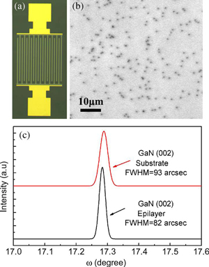 The dislocation density in the GaN layer was measured via cathodoluminescence (Figure 1b) as 5x10⁶/cm2, which compares very favorably with values of 108–1010/cm2 normally found with GaN layers grown on sapphire and silicon carbide substrates (heteroepitaxy).
Figure 1. (a) Photograph of the GaN MSM APD. (b) Panchromatic CL mapping image of homoepitaxial GaN layer grown on bulk GaN substrate. (c) GaN (002) XRD rocking curves of the original bulk GaN substrate and the homoepilayer.
X-ray diffraction (XRD) rocking curves confirmed the material quality with low full-width at half maximum (FWHM) values for the (002) peak of the epilayer and substrate (Figure 1c). The smaller FWHM of the epilayer indicates that it is of higher crystal quality than the substrate. Atomic force microscopy (AFM) measurements over a square region of 5μm gave a surface roughness of ~5nm.
Another problem with nitride diodes is producing p-type material, since the main technique for this — magnesium doping — is not that effective, compared with the silicon doping used to provide n-type material. Avalanche photodiodes that use p-type/intrinsic (i.e. no doping)/n-type (p-i-n) structures produced on free-standing GaN have achieved 104 multiplication gain. However, the presence of the acceptor levels in the p-type material leads to an enhanced red-shift of the absorption edge of the device at high reverse bias.
The Chinese group instead used metal–semiconductor–metal structures, depending on the Schottky diode rectifying effect that occurs at metal–semiconductor interfaces. Interdigitated Schottky electrodes were defined by photolithography and lift-off (Figure 1a). The electrodes used a semi-transparent nickel-gold (5nm/5nm) stack. The electrode fingers were 10μm wide and 400μm long. The spacing was 10μm. An evaporated 200nm titanium-gold layer was patterned into contact pads.
Dark current and photocurrent under 6.5μW/mm2 365nm UV illumination were measured (Figure 2). The dark current at 20V bias was 8.8pA (1.4x10⁻⁹A/cm2 density). At higher bias there is a rapid increase in dark current that could be attributed to bulk dislocation defects or surface states that remain in the GaN crystal. The photocurrent tends to saturate around 20V.
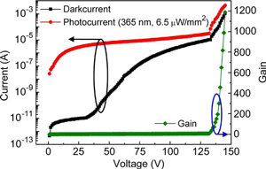 Figure 2. Current vs voltage (I–V) characteristics of APD measured under dark and under 365nm light illumination. Calculated avalanche gain of APD as function of bias is also shown.
At around 130V avalanche breakdown begins, as shown by increases in both photo- and dark-current. The gain was calculated based on the current values at 20V, where saturation of the unmultiplied photocurrent occurs. The gain at 145V is estimated to be 1188, which is a lower value than some GaN p-i-n APDs reported.
The cut-off of photo-response occurs around a wavelength of about 365nm that corresponds to the energy bandgap of the GaN material (~3.4eV). As the bias increases, there is an undesired red-shift of the cut-off, probably due to the Franz–Keldysh effect where the electron and hole wavefunctions become modified by the electric field so they can overlap and couple with photons in classically forbidden areas. The rejection ratio of 360nm UV over 450nm blue light is ~105 at 20V bias. Variation of the performance with temperatures up to 425K was used to rule out other mechanisms for the photo-multiplication such as temperature-insensitive Zener tunneling.
Device simulations were used to estimate the critical electric field where breakdown begins, giving a value of 3.4MV/cm, agreeing with the theoretical breakdown field of GaN. The researchers believe they could improve the gain and stability of the avalanche breakdown with a new device design. Such a design would aim to create more uniform avalanche breakdown beneath the semi-transparent cathode, possibly using field-averaging schemes such as through adding a field-plate to modify the electric field pattern in the GaN material.
The author Mike Cooke is a freelance technology journalist who has worked in the semiconductor and advanced technology sectors since 1997.