- News
14 December 2011
Jenoptik lays foundation stone for €10m extension of Berlin plant
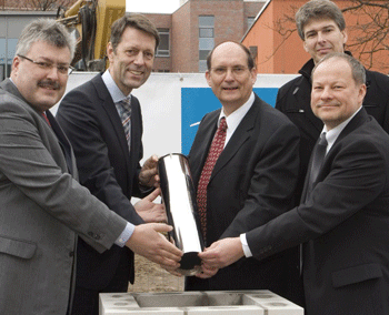 In a ceremony attended by about 80 invited guests (including representatives from business, politics and industry), Jenoptik Group of Jena, Germany has laid the foundation stone for the €10m expansion that will more than double capacity at its gallium arsenide (GaAs)-based high-power semiconductor laser production site in the Berlin-Adlershof technology park.
“Germany is and remains a location for high-tech manufacturing even though we in the Jenoptik Group are currently pushing forward the process of internationalization in Asia and North America,” said Jenoptik chairman Dr Michael Mertin, emphasizing the need for investment primarily in technology-intensive fields. “Our local industry knows how to position itself as a supplier of high-tech to the world,” he added.
The existing production facility in Berlin has reached its capacity limit and is being expanded due to rapidly increasing demand (particularly from Asia), as well as for future projects, including the progressing internationalization of the firm’s Lasers & Material Processing division.
The expansion will increase total floor area by 1400m2 to about 3400m2. The production area, including cleanroom, will grow from 540m2 to 930m2. A topping-out ceremony is scheduled for 5 March 2012, prior to building handover from Stuttgart-based general contractor YIT Germany GmbH in the Summer. The plant should be available for production from 2013.
After the manufacturing facility has been equipped with production and automation technology, 4-inch GaAs wafers will be structured and processed to create high-power laser bars in a typical semiconductor manufacturing process. The various work areas will be fitted out with Class 100-1000 cleanroom facilities (depending on the requirements of the specific process step). The complete process line - from epitaxy, wafer processing and facet coating through to the manufacture of GaAs components - will be installed in the cleanrooms.
A total of about €10m is being invested in the extension. Financing for the building will be provided by the Hoesch Dortmund pension fund. The internal fittings (including cleanrooms) as well as the production equipment will come from Jenoptik. Including the existing production facility, total investment at the Berlin-Adlershof site will be about €24m.
Laser bars from the Berlin-Adlershof plant will be shipped to customers worldwide and will also be processed to create high-power diode lasers by Jenoptik in Jena, where it has the entire technology chain at its disposal - from the manufacture of high-power diode lasers (the most energy-efficient of all lasers), through to laser processing systems for material processing.
Jenoptik has had its own production facility in Berlin-Adlershof since 2006. The optoelectronic base material and its efficient production are being developed by Jenoptik in close collaboration with the Ferdinand-Braun-Institute, Leibniz Institute for High Frequency Technology (FBH) in Berlin-Adlershof. Currently Jenoptik employs 70 people in Berlin, mainly in the Lasers & Material Processing and Optical Systems divisions. As a result of the investment, staffing will rise by 2013, in accord with expected future growth.
Jenoptik investing €10m to double production of GaAs laser bars