- News
20 December 2011
Creating high-performance nitride semiconductor MOSFETs on silicon
National Chiao Tung University has used lanthanum aluminate (LaAlO3) and silicon dioxide (SiO2) dielectric layers to create nitride semiconductor metal-oxide semiconductor field-effect transistors (MOSFETs) on silicon substrates [C. Y. Tsai et al, IEEE Electron Device Letters, published online 25 November 2011]. The LaAlO3 allowed high-dielectric-constant (κ) layers to be formed.
The devices achieved a record normalized drive current (mobility x oxide capacitance) of 172μA/V2. The on-resistance was a low 13.5Ω-mm2 at a gate voltage +2V, and the transconductance was high at 136mS/mm. Breakdown occurred at 385V with a gate potential of –1V.
The use of an insulated gate allows a positive threshold voltage (Vt), unlike nitride semiconductor transistors with a Schottky gate that usually have negative threshold. The researchers aimed at a low Vt value to match the needs of smart power control using silicon CMOS drivers that operate below 1V. With a drain bias of 3V, the threshold of the nitride MOSFET was +0.1V and the peak transconductance was 136mS/mm. The on/off drive current ratio was 76. The subthreshold slope was 0.53V/decade.
The subthreshold slope (SS) was one of the most favorable among the insulated-gate GaN devices reported so far (Table 1), but is much higher than that achieved with silicon and needs to be improved. The researchers suggest that using lightly doped p-GaN would be one way to do this.
|
Gate dielectric |
Vt (V) |
Ron (Ω-mm) |
Ion/loff |
SS (V/dec) |
Mobility (cm2/V-s) |
gm,max (mS/mm) |
μCox (μA/V2) |
Breakdown voltage (V) |
This Work |
LaAlO3/SiO2 |
0.1 |
13.5 (Vg = 2V) |
76 |
0.53 |
201 |
136 |
172 |
385 |
Ion-implanted MOSFET |
SiO2 |
2.7 |
700 (Vg =34V) |
1667 |
3.4 |
45 |
6 |
0.38 |
700 |
Ion-implanted MOSFET |
SiO2 |
3.3 |
90 (Vg = 30V) |
1250 |
0.49 |
167 |
- |
2.87 |
- |
MOSHEMT w. SAG |
SiO2 |
2.1 |
62.5 (Vg =20V) |
2x10⁶ |
0.75 |
113 |
- |
3.72 |
60 |
MOSHEMT |
PEC SiO2 |
-5 |
16 (Vg. =2V) |
- |
1.35 |
- |
50 |
27.8 |
|
Gate-recessed MISFET |
Si3N4 |
5.2 |
25 (Vg =13V) |
- |
8.64 |
120 |
- |
- |
400 |
RFSURF MOSFET |
SiO2 |
-0.5 |
135 (Vg = 30V) |
- |
- |
120 |
- |
7.3 |
730 |
Gate-recessed MOSFET |
Al203 |
2 |
9.7 (Vg = 6V) |
- |
0.9 |
225 |
98 |
6.25 |
40 |
Gate-recessed MISHEMT |
Al203 |
3 |
6.2 (Vg = 10V) |
- |
1.31 |
- |
155 |
13.7 |
320 |
lon-implanted MOSFET |
TiO2-MgO/MgO |
1.3 |
62.5 (Vg = 8V) |
3500 |
0.34 |
13 |
- |
1.49 |
- |
Table 1: Comparison of crucial device characteristics of GaN MOSFETs.
Increasing the on/off ratio is a particular challenge for GaN MOSFETs. Although gate recessing is used to increase its value, beyond a certain point the channel becomes broken, causing device failure. Therefore, one seeks ways to reduce the off-state leakage current.
Possible strategies include reducing the background n-type doping, using an InAlGaN buffer consisting of a tuned combination of four elements (quaternary), or thinning the GaN buffer thickness. The researchers believe that the peak transconductance and on-current values could be increased by reducing the gate–source spacing.
The aluminum gallium nitride/gallium nitride (AlGaN/GaN) epitaxial structures were grown on (111) silicon, resulting in a material with two-dimensional electron gas (2DEG) of carrier density
1.08x10¹³/cm2 and mobility 1458cm2/V-s. The growth began with 2.4μm low-temperature deposited GaN, followed by 1.2μm GaN channel, 30nm Al0.25Ga0.75N barrier, and 2nm GaN cap.
Mesa structures were etched using a mix of boron trichloride and chlorine plasmas. The gate was recessed using a timed etch and measurement of the source–drain current of ungated devices. The recess was cleaned and then the gate dielectric of 1.5nm SiO2 and 6.5nm LaAlO3 was deposited using electron-beam evaporation at room temperature.
“The interfacial SiO2 is vital for achieving favorable high-κ MOSFET performance with low Vt,” the researchers comment.
The deposition was followed by annealing at 400°C for 5 minutes in oxygen. The aim of the anneal step was to improve the quality of the dielectric layers and the interface with the underlying GaN.
The source–drain regions were then defined and formed by removing the dielectric stack with a reactive-ion etch process. The ohmic source–drain electrodes consisted of titanium/aluminum/titanium/gold. The 5μm-long gate was nickel-gold. The gate width was 100μm. The gate was positioned with drain- and source-spacing of 10μm and 5μm, respectively.
Capacitance–voltage measurements on the gate structure gave a capacitance equivalent thickness (CET) of 3nm. The peak mobility of 201cm2/V-s is described as one of the most favorable results for GaN MOSFETs. This value falls far short of the 1458cm2/V-s found for the 2DEG at AlGaN/GaN measured before dielectric deposition.
The difference is attributed to dielectric/GaN interface scattering. However, the mobility degradation at high effective electric field is considerably slower than for silicon-based devices (Figure 1), probably due to the lower carrier effective mass in nitride semiconductors (~0.2x mass electron in GaN, ~0.26x in Si). “This trait is a strong merit of the GaN nMOSFET,” the researchers comment.
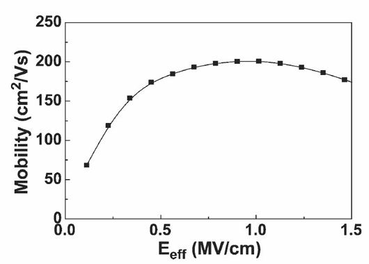
Figure 1: Mobility as a function of effective field of gate-recessed GaN MOSFETs with high-κ
LaAlO3/SiO2 dielectric.
The author Mike Cooke is a freelance technology journalist who has worked in the semiconductor and advanced technology sectors since 1997.