- News
28 December 2011
Metal-assisted chemical etching makes high-aspect-ratio wet etch easier
Led by electrical and computer engineering professor Xiuling Li and supported by the US Department of Energy and the National Science Foundation (NSF), a team of researchers at University of Illinois (UI) has developed a method that should make it easier to chemically etch patterned arrays in gallium arsenide for high-end optoelectronic devices (‘Formation of High Aspect Ratio GaAs Nanostructures With Metal-Assisted Chemical Etching’, Nano Letters).
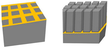 Picture: Metal-assisted chemical etching uses two steps. A thin layer of gold is patterned on top of a wafer with soft lithography (left). The gold catalyzes a chemical reaction that etches the semiconductor from the top down, creating 3D structures for optoelectronic applications (right). (Graphic by Xiuling Li).
Semiconductors are commonly etched with two techniques: wet etching uses a chemical solution to erode the semiconductor in all directions, while dry etching uses a directed beam of ions to bombard the surface, carving out a directed pattern. Such patterns are required for high-aspect-ratio nanostructures (with a large ratio of height to width), which are essential to many high-end optoelectronic device applications. Unfortunately, these materials can be difficult to dry etch, as the high-energy ion blasts damage the semiconductor’s surface (and III-V semiconductors are especially susceptible to damage).
To address this problem, Li and her group turned to metal-assisted chemical etching (MacEtch), a wet-etching approach that they had previously developed for silicon. Unlike other wet methods, MacEtch works in one direction, from the top down. It is faster and less expensive than many dry etch techniques, says Li. Her group revisited the MacEtch technique, optimizing the chemical solution and reaction conditions for GaAs.
The process has two steps. First, a thin film of metal is patterned on the GaAs surface. Then, the metal-patterned semiconductor is immersed in the MacEtch chemical solution. The metal catalyzes the reaction so that only the areas touching metal are etched away, and high-aspect-ratio structures are formed as the metal sinks into the wafer. When etching is completed, the metal can be cleaned from the surface without damaging it.
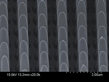 Picture: A scanning electron microscope image of 'nanopillars' etched in GaAs. (Image by Xiuling Li).
“The realization of high-aspect-ratio III-V nanostructure arrays by wet etching can potentially transform the fabrication of semiconductor lasers where surface grating is currently fabricated by dry etching, which is expensive and causes surface damage,” Li says.
To create metal film patterns on the GaAs surface, Li’s team used a patterning technique pioneered by John Rogers, the Lee J. Flory-Founder Chair and a professor of materials science & engineering. Their research teams joined forces to optimize the method (soft lithography) for chemical compatibility while protecting the GaAs surface. Soft lithography is applied to the whole semiconductor wafer, as opposed to small segments, creating patterns over large areas – without expensive optical equipment.
“The combination of soft lithography and MacEtch make the perfect combination to produce large-area, high-aspect-ratio III-V nanostructures in a low-cost fashion,” says Li, who is affiliated with the Micro and Nanotechnology Laboratory, the Frederick Seitz Materials Research Laboratory, and the Beckman Institute for Advanced Science and Technology at UI.
Next, the researchers hope to further optimize conditions for GaAs etching and establish parameters for MacEtch of other III-V semiconductors. They then hope to demonstrate device fabrication, including distributed Bragg reflector (DBR) lasers and photonic crystals. “MacEtch is a universal method as long as the right condition for deferential etching with and without metal can be found,” Li says.
http://pubs.acs.org/doi/full/10.1021/nl202708d