- News
2 February 2011
Superlattice nitride solar cells achieve higher conversion
Meijo and Nagoya universities have extended work on nitride semiconductor solar cells, improving performance through superlattice structures [Yousuke Kuwahara et al, Appl. Phys. Express, vol4, p021001, 2011]. Previous work by the group includes using free-standing gallium nitride (GaN) substrates (Free-standing GaN substrate improves nitride solar cell performance). In that work, the conversion efficiency of such devices was 1.41%. This has now been increased to 2.5% for air mass 1.5G (AM1.5G) standard earth surface solar illumination.
The type of device used covers only a tiny part of the solar spectrum, so the 2.5% conversion efficiency figure is considered high for present nitride-based solar devices. The maximum external quantum efficiency (EQE) was 59.1% for the best device.
To make significant inroads into the rest of the solar spectrum, high-quality growth methods of high-indium-content (> 20%) gallium indium nitride (GaInN) are needed. Such growth methods are also desirable for longer-wavelength nitride semiconductor light-emitting devices (LEDs and lasers) that are also being worked on by many groups, particularly green lasers.
It has been estimated that if high In-content nitride semiconductors could be produced, a four-junction nitride semiconductor solar cell sensitive to different parts of the solar spectrum could have a conversion efficiency of 62%. Further potential advantages of nitride solar cells are radiation hardness, high thermal conductivity and high light absorption. These features would enable deployment in harsh environments such as space and deserts.
The Meijo/Nagoya researchers used metal-organic chemical vapor deposition (MOCVD) on free-standing c-plane GaN substrates (dislocation density less than 107/cm2) to create their epitaxial layers. Trimethyl-indium and -aluminum, along with triethyl-gallium were used as metal sources. The nitrogen came from ammonia (NH3).
One problem in using GaInN for active layers in solar cells is that misfit dislocations tend to form in thick layers. When a Ga0.8In0.2N layer is on GaN, the critical thickness is of the order 1nm, and the resulting dislocations lead to pits at interfaces that degrade solar cell performance. However, thicker layers would be needed to absorb sufficient sunlight.
The Meijo/Nagoya researchers produced devices using a number of thin layers (superlattices) to overcome this problem. The researchers comment: “This is the first time that thick GaInN-based superlattices have been used as an active layer in solar cells to the best of our knowledge.”
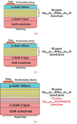 Three devices were produced (Figure 1) with various combinations of superlattice. All devices (A-C) had well/barrier combinations of Ga0.83In0.17N/Ga0.93In0.07N, but the final device (C) had an extra silicon-doped superlattice of Ga0.90In0.10N/GaN next to the n-contact region.
Figure 1: Sample structures. (a) Sample A: GaInN-based solar cell with 50 well/barrier layer pairs of Ga0.83In0.17N (3nm)/Ga0.93In0.07N (3nm) as superlattice active layer. (b) Sample B: GaInN-based solar cell with 50 pairs of Ga0.83In0.17N (3nm)/Ga0.93In0.07N (0.6nm). (c) Sample C: Sample B with 10 additional well/barrier pairs of Ga0.90In0.10N:Si (3nm)/GaN:Si (3nm) ([Si] doping concentration in both cases 3x10¹⁸/cm3).
The ohmic p-contact consisted of semi-transparent nickel-gold (5nm each), while the n-contact consisted of the combination titanium-aluminum-titanium-gold.
Samples A and B (i.e. without silicon-doped superlattice) were studied first. Sample B, with thin barriers, had a very high pit density, but its maximum external quantum efficiency (EQE) was about 15x that of A (Table 1). Also, the open-circuit voltages (Voc) and close-circuit current density (Jsc) were high/low and low/high for samples A and B, respectively. One effect of the high pit density is to increase leakage current, reducing Voc.
Sample |
Voc |
Jsc |
FF |
Max-EQE |
Pit density |
RS |
RSH |
(V) |
(mA/cm2) |
(%) |
(%) |
(x106/cm2) |
( Ω-cm2) |
(x103 Ω-cm2) |
|
A |
1.83 |
0.37 |
50.6 |
3.5 |
15 |
915 |
12.5 |
B |
0.93 |
3.19 |
53.3 |
46.1 |
870 |
50.6 |
2.15 |
C |
1.78 |
3.08 |
70.8 |
59.1 |
< 1 |
50.2 |
12.5 |
Table 1: Voc, Jsc, fill factor (FF), max-EQE, pit density, and series (RS) and shunt (RSH) resistance for samples A-C.
 Sample C was created to combine the good features of the two devices. In particular, sample C has an extra silicon-doped superlattice with thick barriers to reduce the dislocation density, with the aim of improving the material quality of the subsequently grown active region with thin barriers. The resulting material has a pit density of less than 106/cm2, compared with 1.5x10⁷/cm2 for sample A and 8.7x10⁸/cm2 for sample B.
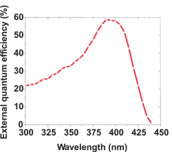
Figure 2: EQE spectra of sample C. EQE reached a maximum of 59% at 390nm wavelength.
The maximum EQE for sample C (Figure 2) was 59.1% at 390nm (violet). At this wavelength, the p-electrode has an estimated transparency of 67%, so the internal quantum efficiency is estimated to be 88%. University of California Santa Barbara (UCSB) recently reported an EQE of 72% at a similar wavelength (Nitride solar cell achieves peak EQE of 72%).
Texas Tech ‘significantly’ improves InGaN solar cell performance