- News
7 January 2011
Free-standing GaN from lateral overgrowth and chemical etch
Researchers from Gwangju Institute of Science and Technology and Samsung LED in Korea have developed a technique to chemically separate laterally overgrown gallium nitride (GaN) crystal from its sapphire substrate [Chu-Young Cho et al, Appl. Phys. Express, vol4, p012104, 2011]. Such ‘free-standing’ GaN is an attractive substrate for growing more efficient light-emitting structures.
Commercial nitride semiconductor light-emitting diodes (LEDs) are generally produced by growing epitaxial layers on sapphire substrates. Since sapphire is electrically insulating, one has to put the device contacts on the nitride semiconductor side of the device. This creates lateral current flows that suffer from current crowding, which reduces efficiency. By removing the sapphire substrate, one is able to put the contacts on both the top and bottom of the device, enabling ‘vertical’ current flow.
Laser-lift off techniques have been developed to remove the sapphire, but can cause strain-induced cracking and other damage of the device structure, impacting performance. Another approach is chemical, where defects are not expected to be generated since physical and thermal damage are avoided.
The Gwangju Institute of Science and Technology and Samsung LED combined chemical lift-off and lateral epitaxial overgrowth (LEO, also known as epitaxial lateral overgrowth/ELOG). LEO uses a mask to block threading dislocations in certain parts of the GaN template, creating regions of near-damage-free crystal from material that grows over the mask.
The technique begins with growing GaN seed layers on c-plane sapphire using metal-organic chemical vapor deposition (MOCVD). A 25nm GaN nucleation layer (grown at 550°C) was followed by 2μm-thick undoped GaN (1020°C).
The LEO process was performed using silicon dioxide coated tungsten as a mask that consisted of a series of lines 6μm wide with 6μm gaps (Figures 1a and b). The 8μm-thick LEO GaN layer was grown at 1020°C (Figures 1c and d).
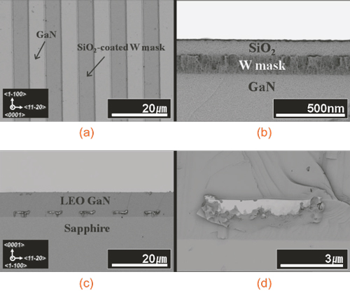
Figure 1: (a) Plan-view and (b) cross-sectional SEMs of SiO2-coated W mask. (c), (d) Cross-sectional SEMs of LEO GaN epilayer grown on the SiO2-coated W mask.
The voids that are seen under the LEO mask are attributed to GaN decomposition reactions involving GaN, tungsten, and the hydrogen gas that was used as carrier during the MOCVD growth.
The LEO GaN was separated from the sapphire using a molten potassium hydroxide (KOH) etch (150°C for 10–60 minutes) of the GaN between the voids (Figure 2). The researchers believe that the KOH penetrates the voids and then etches the remaining template GaN.
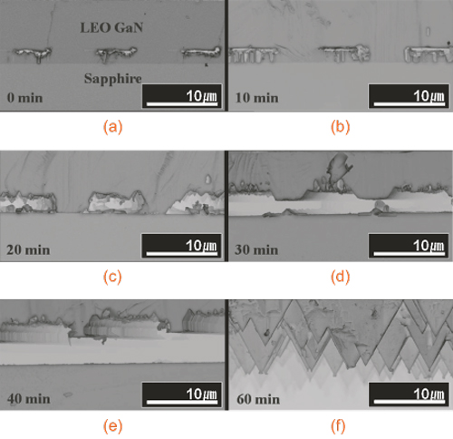
Figure 2: Cross-sectional SEMs of (a) LEO GaN epilayer before etching process; and (b–f) LEO GaN epilayers etched in the KOH for 10–60 minutes.
The etched surface was covered with inverted pyramids (Figure 2f). Such surface texturing has been used in GaN LEDs to reduce total internal reflection effects where photons are reflected back into the device at air–GaN interfaces.
Various analyses of the separated GaN were carried out to check the material quality. Transmission electron micrography (TEM) showed that the SiO2/W mask had effectively prevented propagation of the threading dislocations from the lower template layers. By contrast, threading dislocations were seen in the gaps/windows in the mask. Atomic force microscopy (AFM) showed reduced surface roughness above the mask (0.37nm root mean square) compared with the window region (0.52nm RMS). Surface pits formed from threading dislocations had a density of 5x10⁷/cm2 in the mask regions, which increased to 2x10⁹/cm2 in the window regions.
Photoluminescence (PL) and Raman spectroscopy measurements were also performed. The PL intensity for the LEO GaN was increased by 63% compared with as-grown samples without LEO. The improvement is attributed to reduced dislocation densities.
Raman spectroscopy probes the phonon spectrum, which is related to vibration modes of the lattice through energy shifts in photon scattering. Vibration modes are affected by changes in strain.
The LEO GaN had a Raman peak red-shifted relative to the as-grown material. The value obtained (1.2/cm in wavenumbers) suggests a compressive stress relaxation of 0.285GPa. This relaxation is attributed to the void formation process.
Free-standing GaN substrates LEDs Lateral epitaxial overgrowth
http://apex.jsap.jp/link?APEX/4/012104
www.samsungled.com/eng/main/index.asp
http://mse1.gist.ac.kr/eng/persons/view/professor/37
The author Mike Cooke is a freelance technology journalist who has worked in the semiconductor and advanced technology sectors since 1997.