- News
27 January 2011
Multi-band GaAsN cell yields full-spectrum solar response
Researchers from the Materials Sciences Division (MSD) of the US Department of Energy’s Lawrence Berkeley National Laboratory — as well as Rose Street Labs Energy and Sumika Electronic Materials Inc (both of Phoenix, AZ) — have demonstrated a solar cell that not only responds to almost the entire solar spectrum but can readily be made using common low-cost semiconductor industry manufacturing techniques (‘Engineering the Electronic Band Structure for Multiband Solar Cells’, Nair Lopez, Lothar Reichertz, Kin Man Yu, Ken Campman and Wladyslaw Walukiewicz, Phys. Rev. Lett. 106, 028701 (2011), 10 January).
Although full-spectrum solar cells have been made previously, none have yet been suitable for manufacture at a consumer-friendly price. However, the new design promises highly efficient solar cells that are practical to produce, say the researchers.
Since solar cells are made from semiconductors that absorb most efficiently at wavelengths corresponding to energies above its bandgap (the energy it takes to excite an electron from the valence to the conduction band), no single semiconductor material can absorb sunlight’s full range of wavelengths (from low-energy infrared through visible light to high-energy ultraviolet).
“The underlying principle of a successful full-spectrum solar cell is to combine different semiconductors with different energy gaps,” says Wladek Walukiewicz, who leads the Solar Energy Materials Research Group in Lawrence Berkeley’s MSD.
One way to combine different bandgaps is to stack layers of different semiconductors and wire them in series (the principle behind existing high-efficiency solar cells that uses three different semiconductor alloys with different bandgaps). In 2002, Walukiewicz and Kin Man Yu of Berkeley Lab’s MSD found that, by adjusting the amounts of indium and gallium in the same alloy (indium gallium nitride), each different mixture responded to different wavelengths. By stacking several crystalline layers, all closely matched but with different indium content, they made a photovoltaic device that was sensitive to the full solar spectrum.
However, “Even when the different layers are well matched, these structures are still complex — and so is the process of manufacturing them,” says Walukiewicz. “Another way to make a full-spectrum cell is to make a single alloy with more than one band gap.”
In 2004 Walukiewicz and Yu made an alloy of highly mismatched semiconductors based on a common alloy, zinc (plus manganese) and tellurium. By doping this with oxygen, they added a third distinct energy band between the existing two, creating three different bandgaps that spanned the solar spectrum. Unfortunately, says Walukiewicz, “to manufacture this alloy is complex and time-consuming, and these solar cells are also expensive to produce in quantity.”
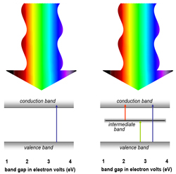
 Figure 1: A solar cell’s efficiency is limited by its semiconductor bandgap energy: a wide bandgap responds to shorter wavelengths with higher energies (lower left); an intermediate band has multiple bandgaps and can respond to a range of energies (lower right).
The latest solar cell material is another multi-band semiconductor made from a highly mismatched alloy, in this case gallium arsenide nitride (GaAsN), which is similar in composition to the familiar gallium arsenide and likewise able to be made using the conventional method of metal-organic chemical vapor deposition (MOCVD).
By replacing some of the arsenic atoms with nitrogen, a third, intermediate energy band is created between the material’s valence band and conduction band. Hence, the same basic material becomes a multi-band semiconductor.
So, compared with the wide bandgap between the valence band and conduction band that allows high-energy (i.e. short-wavelength) transitions, there is a narrow bandgap between the valence band and the intermediate band that allows transitions at low-energy (i.e. long-wavelength), and between the intermediate band and the conduction band there is a slightly less narrow bandgap that responds to intermediate-energy transitions (i.e. intermediate wavelengths).
“The major issue in creating a full-spectrum solar cell is finding the right material,” says Kin Man Yu. “The challenge is to balance the proper composition with the proper doping.”
Finding the right combination of alloys, and determining the appropriate doping levels to put an intermediate band just where it’s needed, is mostly based on theory, using the band anti-crossing model of the electronic structure of highly mismatched alloys that was developed at Berkeley Lab over the past 10 years. “We knew that 2% nitrogen ought to do the job,” says Yu. “We knew where the intermediate band ought to be and what to expect. The challenge was designing the actual device,” he adds.
Using the new multi-band material as the core of a test cell, the researchers illuminated it with the full spectrum of sunlight to measure how much current was produced by different colors of light. The key to making a multi-band cell work is to make sure that the intermediate band is isolated from the contacts where current is collected. “The intermediate band must absorb light, but it acts only as a stepping stone and must not be allowed to conduct charge, or else it basically shorts out the device,” Walukiewicz explains.
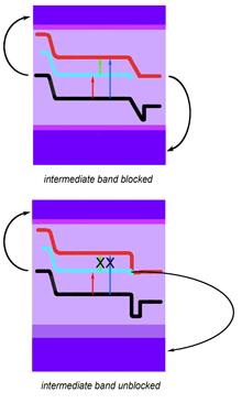
 Figure 2: Top: a test device of the multiband solar cell arranged to block current from the intermediate band, allowing a wide range of wavelengths to stimulate current from both conduction and valence bands (electrons and holes, respectively). Bottom: current from the intermediate band unblocked, and interfering with current from the conduction band, limiting response.
The test device had negatively doped semiconductor contacts on the substrate to collect electrons from the conduction band, and positively doped semiconductor contacts on the surface to collect holes from the valence band. Current from the intermediate band was blocked by additional layers on top and bottom.
For comparison purposes, the researchers built a cell that was almost identical but not blocked at the bottom, allowing current to flow directly from the intermediate band to the substrate.
The results of the test showed that light penetrating the blocked device efficiently yielded current from all three energy bands — valence to intermediate, intermediate to conduction, and valence to conduction — and responded strongly to all parts of the spectrum, from infrared (with an energy of about 1.1eV) to well into the ultraviolet (more than 3.2eV).
By comparison, the unblocked device responded well only in the near infrared, declining sharply in the visible part of the spectrum and missing the highest-energy sunlight. Because it was unblocked, the intermediate band had essentially usurped the conduction band, intercepting low-energy electrons from the valence band and shuttling them directly to the contact layer.
Further support for the success of the multi-band device and its method of operation came from tests ‘in reverse’, i.e. operating the device as a light-emitting diode. At low voltage, the device emitted four peaks in the infrared and visible light regions of the spectrum. Primarily intended as a solar cell material, this performance as an LED may suggest additional possibilities for GaAsN, since it is a dilute nitride very similar to the dilute nitride InGaAsN (indium gallium arsenide nitride) that is used in commercial vertical-cavity surface-emitting lasers (VCSELs), which have found widespread use because of their advantages over other semiconductor lasers.
The research team says that, with the new GaAsN-based multi-band photovoltaic device, it has demonstrated a simple solar cell that responds to almost the entire solar spectrum, and can readily be fabricated using one of the semiconductor industry’s most common manufacturing techniques (MOCVD). The results promise highly efficient solar cells that are practical to produce, they add.
