- News
27 January 2011
 Exploring droop and wide-well nitride LEDs
Researchers in Taiwan have been exploring efficiency droop effects in wide-well light-emitting diodes (LEDs) [Liann-Be Chang et al, Appl. Phys. Express, vol4, p012106, 2010]. Such effects have been widely studied for LEDs that use thin multi-quantum wells (2–4nm), but not so much for wider single-well double heterostructures (DHs).
The results of the researchers’ work suggests “that the electron leakage significantly decreases the peak EQE [external quantum efficiency] and shifts the start point of efficiency drop to a higher current density, but is not significantly responsible for the efficiency droop in the wide-well InGaN DH LEDs”. The researchers conclude: “Thus, we suggest that the hole injection efficiency probably dominates the mechanism of efficiency droop rather than electron leakage”.
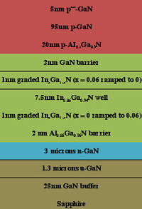
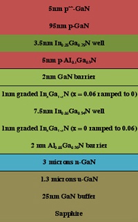
Figure 1: Schematic structures of samples LED-1 (right, top) (reference LED structure) and LED-2 (right, bottom) (leakage test LED structure).
 The researchers at Chang Gung University produced two structures (Figure 1). The first (LED-1) was a single-well device with a 7.5nm well. The device also incorporated a 20nm electron-blocking layer (EBL) consisting of p-type conducting AlGaN (10% Al). EBLs are used to reduce overflow of electrons from the active region into the p-contact region. Such overflow diverts electrons from recombining directly with holes in the active region, reducing light emission.
The second structure (LED-2) was the same, except that the EBL was thinned to 5nm and an extra 3.5nm InGaN well was inserted between the EBL and p-contact layers. (The researchers found that devices with a test structure and a 20nm EBL did not have sufficient overflow to give emission from the test well.) The purpose of this well was to detect (through light emission) overflow electrons that evade the EBL. Having a higher indium content (25%) compared with the main well (6% In), one would expect the extra well to emit at longer wavelengths.
The epitaxial structures were produced on sapphire substrates using atmospheric-pressure metal-organic chemical vapor deposition (AP-MOCVD). The epitaxial material was processed into 295μm x 325μm LEDs by standard processes. A 300nm indium tin oxide (ITO) was used to spread the current below the p-electrode. The metal combination used for the electrodes was chromium-platinum-gold.
 The electroluminescence (EL) tests were carried out at room temperature with pulsed operation (100μsec pulse, 1% duty cycle) to avoid self-heating effects. The light output through the ITO film was measured.
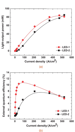
The researchers found that the effect of the thinner EBL, allowing greater electron leakage into the contact region (but also better hole injection into the wide well), was to reduce the peak efficiency (Figure 2). However, the efficiency droop kicked in at a higher injection current (208.6A/cm2, compared with 83.4A/cm2 for LED-1) and was less steep than for the thicker EBL of the device without test structure.
Figure 2: (a) Light-output power of samples LED-1 and LED-2 vs forward current density. (b) EQE of samples LED-1 and LED-2 vs forward current density.
Another interesting feature is that the light output power of LED-2 exceeds that of LED-1 when the current injection is greater than 500A/cm2.
In terms of the output spectrum (Figure 3), the test structure showing electron overflow can be seen as another peak in the wavelength region 480–520nm (blue-green). Initially, the test structure peak dominates (up to 3.1A/cm2), but becomes less significant at higher currents as holes begin to reach the wide-well region. 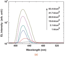
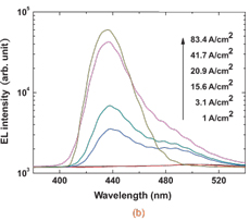
Figure 3: EL spectra with forward current density ranging from 1 to 83.4A/cm2 for samples (a) LED-1 and (b) LED-2.
The author Mike Cooke is a freelance technology journalist who has worked in the semiconductor and advanced technology sectors since 1997.