- News
18 July 2011
Blocking stacking faults with aluminium nitride
Researchers at Otto-von-Guericke-Universität (OVGU) Magdeburg, Germany have been investigating the effect of aluminium nitride (AlN) layers for reducing stacking faults in semi-/non-polar gallium nitride (GaN) crystal structures [A. Dadgar et al, App. Phys. Lett., vol99, p021905, 2011]. The researchers believe that their method “enables low-cost virtually stacking-fault-free semi-polar GaN layers on heterosubstrates and an interesting route for polarization-free long-wavelength LEDs.”
Stacking faults are a roadblock to improved green and longer-wavelength light emission in nitride semiconductor material grown on lower-cost substrates. Semi-/non-polar oriented crystal structures can reduce or eliminate polarization electric fields that pull electrons and holes apart. This ‘quantum-confined Stark effect’ (QCSE) reduces radiative recombination and thus reduces a light-emitting device’s efficiency.
Although semi-/non-polar devices have been developed in the laboratory with longer wavelengths than traditional c-plane devices, the substrate material is presently expensive, using extra processes such as epitaxial lateral over-growth (ELOG) or cutting very small pieces of high-quality nitride semiconductor material from c-plane crystals from hydride vapor phase epitaxy (HVPE) processes. Manufacturers want low-cost production derived from simple processing and inexpensive materials.
The OVGU materials were grown on silicon substrates using metal-organic chemical vapor deposition (MOCVD). By changing the crystal orientation of the substrates, different orientations of nitride semiconductor resulted. Silicon oriented with a (112) surface tilted the c-axis of the hexagonal gallium nitride semiconductor layers about 18°in the [1-100] direction, while Si(113) increased the angle to 22°. The GaN on Si(112) layers were found to be oriented close to (10-16).
The seeding layer consisting of AlN has to be kept very thin to maintain a constant axis tilt. To avoid meltback etching of the nitride layers in the further GaN growth process, Al-rich buffer layers or a layer of low-temperature AlN (LT-AlN) were applied in one set of samples. In other samples, an LT-AlN layer was applied later, after about 600nm. This latter technique was found to reduce basal plane stacking faults (BSFs) in subsequent material. The samples were subjected to cathodoluminescence (CL), scanning transmission electron microscopy (STEM), and STEM–CL analyses.
Previous OVGU work on depositing GaN on high crystal index silicon showed layers with rough pyramidal undulations with (0001) plateaus. LT-AlN layers deposited at an early stage in such growth (sample I) tend to follow these undulations (Figure 1a). The previous work also performed photoluminescence measurements that showed emissions from a bound donor exciton (D0, X) and from strong basal plane stacking fault (BSF), and donor acceptor pair band (DAP) and/or prismatic plane stacking fault (PSF) features.
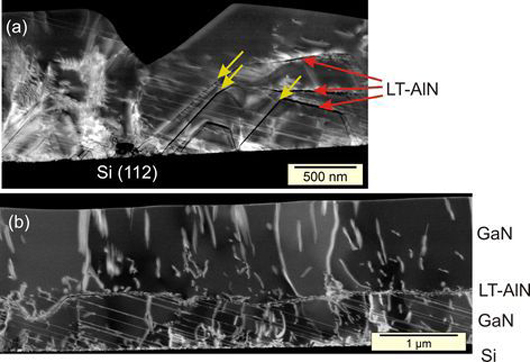
Figure 1: STEM images of sample I (a) and sample II (b). For sample I, the LT-AlN layers are grown during the early ‘island growth mode’. BSFs propagate at an angle of ~18° to the substrate surface and are usually not blocked by the AlN layer (e.g. below yellow arrows). For sample II with an LT-AlN layer grown on a nearly planarized growth surface, BSFs are stopped at the LT-AlN layer but not at positions where it is not parallel to the growth surface as, for example, at a growth pit (left) and also at larger growth steps (not shown).
Inserting LT-AlN later in the growth (sample II), when the GaN is nearly planar (Figure 1b), results in the apparent elimination of local cathodoluminescence from BSF and PSF features in material grown above the LT-AlN (Figure 2). Where the LT-AlN layer is parallel to the substrate surface, STEM–CL images show annihilation of the BSFs — however, where there are interruptions, such as at growth pits or large faceted steps, the faults penetrate through to the upper growth region.
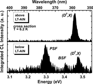 Figure: 2 CL spectra of sample II above and below the LT-AlN layer, demonstrating disappearance of stacking-fault-related luminescence.
The OVGU researchers comment: “The very low density and, on large areas, even the complete absence of BSFs in the upper GaN layer in sample II is a surprising result since LT-AlN layers are only known to lead to lattice relaxation, typically via misfit dislocations at the GaN/LT-AlN interface.”
The team suggests that misfits that eliminate the faults are preferentially produced by the LT-AlN due both to its different lattice constant and higher stacking fault formation energy (0.22mJ/m2). The absence of BSF reduction at growth pits etc could be related to the reduced thickness (~7nm, as opposed to 11nm in planar regions) of the AlN layer in these areas, leading to less lattice relaxation. “Consequently the method requires a critical tensely stressed layer (AlN or AlGaN) thickness to be successful.” The problem in the non-planar regions may also be related to the crystal orientation or inclination angle of the facet surface.
The OVGU group expects the same effect of LT-AlN layers reducing BSFs on m-plane GaN, possibly with an AlGaN grading into GaN after the fault blocking layer. The researchers report that they have not seen any BSF reduction in a-plane material from the use of an LT-AlN layer.
Some funding for the OVGU came from Deutsche Forschungsgemeinschaft (DFG, German Research Foundation) in the framework of the PolarCon research group.
The author Mike Cooke is a freelance technology journalist who has worked in the semiconductor and advanced technology sectors since 1997.