- News
29 July 2011
High-performance 150nm mHEMT on GaAs grown using MOCVD
Researchers at Hong Kong University of Science and Technology (HKUST) have produced high-performance metamorphic high-electron-mobility transistors (mHEMT) with indium aluminum arsenide (InAlAs) barriers and indium gallium arsenide (InGaAs) channels using GaAs substrates and metal-organic chemical vapor deposition (MOCVD) [Haiou Li et al, IEEE Electron Device Letters, published online 22 July 2011].
 InAlAs/InGaAs pseudomorphic HEMT devices on indium phoshide (InP) substrates have achieved cut-off frequencies (fT) of more than 562GHz. Unfortunately, InP substrates remain expensive, in part due to the downturn in the photonic industry after 2000. Hence, it is attractive to explore other ways to produce such high-performance devices, preferably using MOCVD and GaAs substrates.
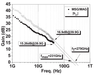
Figure 1: Current gain and MSG/MAG as functions of frequency for HKUST 150nm mHEMT.
The HKUST device has unity current-gain cut-off (fT) and maximum oscillation (fmax) frequencies of 279GHz and 231GHz, respectively (Figure 1). This is comparable to the work of others with InGaAs/InAlAs devices grown with molecular beam epitaxy (MBE) on GaAs or InP (Table 1). The HKUST researchers note that their device has the highest fT yet reported for 150nm gate-length HEMTs.
Sub. |
Growth |
Mob. |
Lg |
Gm |
fT |
fmax |
Date |
|
|
cm2/V-s |
nm |
mS/mm |
GHz |
GHz |
|
GaAs |
MBE |
N/A |
100 |
750 |
154 |
300 |
2004 |
GaAs |
MBE |
N/A |
100 |
890 |
189 |
334 |
2004 |
GaAs |
MBE |
9100 |
150 |
740 |
150 |
240 |
2003 |
InP |
MBE |
8800 |
150 |
800 |
151 |
172 |
2008 |
GaAs |
MBE |
7850 |
100 |
700 |
210 |
N/A |
2005 |
GaAs |
MOCVD |
8740 |
150 |
1074 |
279 |
231 |
2010 |
Table 1: Comparison of AlInAs/GaInAs HEMTs performance. The HKUST device is given in the last row.
The researchers add: “We believe that these results are the best reported for MOCVD-grown mHEMTs and sufficient for high-frequency high-speed applications. With the anticipated demand of commercial high-speed and high-performance transistors, mHEMT technology by MOCVD is very attractive for manufacturing”.
Up to now, metamorphic (i.e. low strain) InAlAs/InGaAs devices on GaAs substrates have been mainly grown using MBE, a technique not favored in manufacturing. MOCVD metamorphic growth has tended to lag behind these developments.
A particular challenge is reducing threading dislocation densities that arise from lattice mismatch (4% between GaAs and InP) and thermal expansion coefficient differences. This is usually handled using a series of buffer layers to bridge the differences in lattice parameters. However, these layers can be less resistive than desired due to unintended impurities, leading to leakage currents in the buffer. These leakage currents hinder the achievement of ‘pinch-off’.
 The HKUST reports: “We have developed a growth technique of a comparatively thin multi-stage buffer to obtain high resistivity in the buffer layer, leading to good device performance. This sets the stage for potential high-volume production of mHEMTs by MOCVD.”
The researchers plan to further reduce buffer leakage by optimizing the buffer layer growth in future.
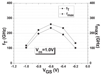
Figure 2: Dependencies of fT and fmax on gate bias for 150nm mHEMTs, where VDS is fixed at 1.0V.
The fT value was derived from short-circuit current gain (|h21|) extrapolation, and de-embedding structures were used to subtract the effect of parasitic capacitance of the probe pads. The fmax value came from extrapolation of maximum stable gain and maximum available gain (MSG/MAG) measurements.
The optimum bias position was determined to be at gate (VGS) and drain (VDS) potentials of –0.6V and 1.0V, respectively (Figure 2).
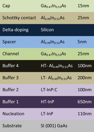 The epitaxial material for the HEMTs (Figure 3) was grown using MOCVD on semi-insulating (SI) 4-inch (001) GaAs substrates. The resulting structure (with cap layer removed for Hall measurements) showed a room-temperature electron concentration in the two-dimensional electron gas (2DEG), which creates the channel, of 4.6x10¹²/cm2 and mobility of 8740 cm2/V-s. These values result in a sheet resistance of 156Ω/sq. Some 60° threading dislocations were observed in the buffer layers.
The devices were made with mesa isolation. The ohmic source/drain contacts consisted of a non-alloyed 6-metal system of nickel-germanium-gold-germanium-nickel-gold with transmission-line method measurements giving contact resistances down to 0.02Ω-mm. The low resistance value is attributed to “higher doping concentration of cap layer and optimization of ohmic contact metal systems”.
Figure 3: Epitaxial metamorphic HEMT structure.
The 150nm T-gate was created using two-stage electron-beam lithography and etch processes on layers of silicon dioxide and silicon nitride deposited using plasma-enhanced chemical vapor deposition. The Schottky gate metal structure on the AlInAs barrier consisted of titanium-platinum-gold.
The device works in depletion-mode (normally-on) with a threshold voltage Vth of about –0.8V. There was some variation in threshold between mHEMT devices in the range from –1.0V to –0.8V. The researchers attribute this to surface roughness, which has a root-mean-square value of more than 2.9nm across a scan area of 20μm x 20μm. It is hoped in future to optimize the growth of the HEMT material to reduce this.
The maximum drain current of the device was 1130mA/mm at a gate potential (VGS) of 0.4V and a drain bias (VDS) of 1.5V. The maximum extrinsic transconductance was found to be 1074mS/mm at VGS of –0.25V and VDS of 1.0V.
The author Mike Cooke is a freelance technology journalist who has worked in the semiconductor and advanced technology sectors since 1997.