- News
13 July 2011
High electron velocity for high HEMT frequencies
HRL Laboratories and University of California San Diego (UCSD) have reported a record cut-off/maximum oscillation frequency (fT/fMAX) combination of 260GHz/394GHz for a nitride semiconductor high-electron-mobility transistor (HEMT) [K. Shinohara et al, IEEE Electron Device Letters, published online 27 June 2011].
The researchers believe that the high-frequency performance benefits from an increasing electron velocity with drain voltage (estimated from delay time-analysis as being at least +24% between 1V and 5V drain bias, and increasing the transconductance 22% from 926mS/mm to 1130mS/mm) “observed here for the first time in a GaN HEMT” due to a combination of aggressive lateral scaling and drain delay suppression. In particular, the source–drain distance was reduced, cutting the drain delay.
In previous HEMT devices, the electron velocity had been limited to less than 1.1x107cm/s, while the theoretical peak expected is more than 2x107cm/s.
The new HRL/UCSD device has a ‘double heterostructure’ (DH-HEMT) with a top and back barrier for the channel (Figure 1). The epitaxial structure was grown on three-inch semi-insulating silicon carbide substrates, using molecular beam epitaxy (MBE). The top barrier was designed to be thin (6nm), while maintaining a high carrier density two-dimensional electron gas (2DEG) and low gate leakage. The back barrier increased carrier confinement and suppressed the effects of having a short gate length (short-channel effects).
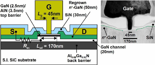
Figure 1: Cross-sectional schematic and TEM image of a laterally scaled 45nm AlN/GaN/Al0.08Ga0.92N DH-HEMT with re-grown n+-GaN ohmic contact.
A sacrificial silicon nitride (SiN) passivation layer, applied using plasma-enhanced chemical vapor deposition (PECVD), boosted the performance of the 2DEG to a carrier density of 1.3x10¹³/cm2 and mobility of 1140cm2/V-s.
The SiN was patterned over the gate region to provide a mask for a chlorine-based reactive ion etch (RIE) designed to cut down through the GaN/AlN top barrier and 10nm of the GaN channel layer for the ohmic contacts that were re-grown as silicon-doped n+-type GaN, again using MBE. The n+-GaN overlapped 0.4μm onto the top barrier layers.
The SiN layer was then removed and non-alloyed titanium-platinum deposited as ohmic source–drain electrodes. Transmission-line method measurements gave a total contact resistance between the ohmic metal and 2DEG channel of 0.1Ω-mm.
A mesa-isolation chlorine-based RIE was followed by a new 30nm layer of PECVD SiN passivation. A 45nm gate foot was patterned and etched on the SiN using carbon tetrafluoride inductively coupled-plasma RIE. The gate metal consisted of platinum-gold. The source–drain distance was 170nm, as defined by the edges of the two regions of re-grown n+-GaN. The gate width was 2x40μm.
The on-resistance was a record low value of 0.44Ω-mm and the maximum output current was ‘high’ at 2.3A/mm. Three-terminal OFF-state breakdown for a source–drain current of 1mA/mm was 13.1V corresponding to an average field of 2.1MV/cm, falling short of the material breakdown field of ~3MV/cm, attributed ‘possibly’ to field non-uniformity.
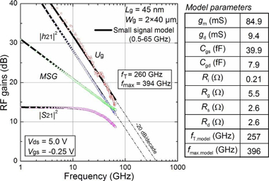 The frequency performance was tested over the range 0.5–65GHz (Figure 2). Parasitic pad capacitance and inductances were de-embedded from the measurements. The peak cut-off and maximum oscillation frequencies were obtained from suitable extrapolations as 260GHz and 394GHz, respectively, at a drain voltage of 5V and a gate potential of –0.25V. The ‘extrinsic’ values, without de-embedding, were 217GHz and 389GHz, respectively.
Figure 2: RF characteristics (0.5–65GHz) of DH-HEMT. Thick solid lines represent simulated RF gains using a small-signal equivalent circuit model with extracted parameters listed in the table.
The RF and DC intrinsic peak transconductances (gm) were consistent at 1060mS/mm and 1130mS/mm, respectively. The peak extrinsic DC transconductance was 905mS/mm.
Funding for the work came from the US Defense Advanced Research Projects Agency (DARPA) Microsystems Technology Office (MTO) Nitride Electronic NeXt-Generation Technology (NEXT) program.
Quaternary nitride HEMT with record cut-off frequency
The author Mike Cooke is a freelance technology journalist who has worked in the semiconductor and advanced technology sectors since 1997.