- News
12 July 2011
Nichia reports first room-temperature blue/‘green’ VCSELs with current injection
Japan’s Nichia Corp has developed room-temperature blue and ‘green’ vertical-cavity surface-emitting lasers (VCSELs) “for the first time, by current injection”, using nitride semiconductor technology for the active region [Daiji Kasahara et al, Appl. Phys. Express, vol4, p072103, 2011].
The thresholds for some of the blue devices (451nm wavelength) and ‘green’ devices (503nm wavelength, actually more blue-green, with true green starting at longer than 520nm) were measured, respectively, as 3.0 and 28kA/cm2 for current density (assuming uniform injection of 1.5 and 22mA over current aperture), and 3.3V and 6.3V for forward voltage. The current apertures for the blue and ‘green’ devices were 8μm and 10μm, respectively.
While the blue device was subjected to continuous-wave (CW) operation, the more challenging green device was only tested under pulsed operation (width/period 1/500μsec). The maximum output power for the blue device was 0.7mW at 11mA. Within the limitations of the pulsed test set-up, the maximum green output power is estimated at more than 0.8mW.
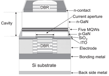 The epitaxial material structures were grown on c-plane gallium nitride (GaN) substrates using metal-organic chemical vapor deposition (MOCVD). The active region consisted of indium gallium nitride (InGaN) wells in GaN barriers. Further processing to make the VCSEL (Figure 1) consisted of a series of steps involving lithography, sputtering, inductively couple plasma (ICP) reactive ion etching, wafer bonding, and chemical mechanical polishing (CMP).
Figure 1: Schematic illustration of structure of blue and green GaN-based VCSELs.
First, a current aperture was patterned, followed by application of an indium tin oxide (ITO) transparent conducting contact and current-spreading layer, then an electrode around the current aperture. The backside mirror consisted of silicon dioxide/niobium pentoxide (SiO2/Nb2O5) layer pairs as a distributed Bragg reflector (DBR). The structure was then flipped and bonded onto a highly conductive silicon substrate. The GaN substrate and n-type layer were then removed/thinned to create suitable cavities before the n-type contact and another SiO2/Nb2O5 DBR.
Further characterization of the devices involved looking at spectra below, near and above threshold and at the near-field emission patterns. The ‘green’ device shifts its wavelength by about 4nm, going from 499nm to 503nm, in moving from spontaneous to stimulated emission. The researchers report: “This abnormal behavior of the laser emission peak may be due to refractive index changes induced by thermal effects. The characteristics of GaN-based VCSELs above 480nm are not well understood and we are currently investigating them.”
 The lasing near-field patterns were found to vary with spot sizes and locations shifting between devices with violet to green emission. The team comments: “We regard this phenomenon to be critical in controlling laser performance. We speculate that it may be related to some kind of inhomogeneity (e.g. material composition, surface morphology, cavity length, current spreading, transverse optical confinement), but it is not possible to make firm conclusions at this stage.”
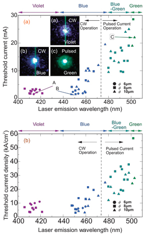
Nichia has produced numbers of devices with various apertures emitting in the ‘green’, blue and violet (Figure 2). The researchers find a trend of increasing threshold currents as the devices become longer wavelength. In general, it is found that devices with wavelengths less than 471nm can sustain room-temperature CW lasing, while those above cannot.
Figure 2: Dispersion diagram for CW operation and pulsed current operation at room temperature. Circles, squares, and triangles indicate results for 6-, 8-, and 10μm-diameter devices, respectively. Insets (a)–(c) show near-field patterns of violet (414nm), blue (451nm), and ‘green’ (503nm) VCSELs corresponding to devices A–C, respectively.
“We speculate that the increase in the threshold current is due to the quantum confinement Stark effect (QCSE) that mainly originates from the piezoelectric polarization caused by the high crystal strain due to the large lattice mismatch between GaN and InGaN. The QCSE is responsible for separating the hole and electron wave-functions, which reduces the radiative recombination probability and thus increases the threshold current.”
The Nichia team believes that ‘green’ thresholds could be reduced, possibly using non- or semi-polar nitride semiconductor structures, as developed by other research groups for edge-emitting lasers.
The researchers conclude: “Many characteristics of GaN-based VCSELs still need to be clarified before reproducible and high-performance GaN-based VCSELs can be fabricated.”
The author Mike Cooke is a freelance technology journalist who has worked in the semiconductor and advanced technology sectors since 1997.