- News
27 July 2011
Hot electrons in nitride semiconductors
University of California Santa Barbara (UCSB) has reported on its first demonstration of hot-electron transistors (HETs) built with the aluminium gallium nitride material system [Sansaptak Dasgupta et al, IEEE Electron Device Letters published online 5 July 2011]
Although nitride bipolar transistors have been made, the difficulties of producing p-type regions and poor conduction properties of holes limit the performance of such devices. The hot-electron transistor is unipolar and can be built based on just n-type electron conduction.
Preliminary simulations on AlGaN/GaN/AlGaN HETs have suggested that up to terahertz performance might be possible eventually. Further motivation for constructing such devices is as a spectroscopic tool for analyzing high-field and high-carrier-velocity effects for devices such as nitride semiconductor high-electron-mobility transistors (HEMTs). Nitride HEMTs are being widely developed for radio-frequency amplification and power switching applications.
In an HET (Figure 1a), electrons are injected over a barrier into a transit region and then collected. Since the electrons that enter the transit region have higher energy than the Fermi level of the transit region, they are labeled ‘hot’. The injection, transit and collection regions are labeled ‘emitter’, ‘base’ and ‘collector’, in line with bipolar transistor terminology.
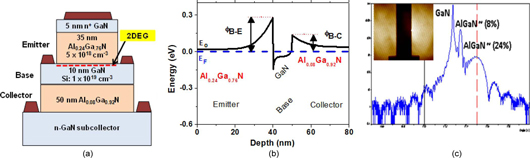
Figure 1: (a) Device structure and (b) band diagram of fabricated HET. (c) High-resolution x-ray diffraction (HRXRD) scan for accurate thickness calibration; and (inset) atomic force micrograph (AFM) after emitter etch.
The potential operating speeds of such devices are high. Unlike in bipolar transistors with various n- and p-type regions, where the main current flow across the base is through minority carriers, the HET is a unipolar structure that uses majority electron carriers. In nitrides, producing the n-type regions with silicon doping is much easier than p-type with magnesium doping, and velocities for electrons are much higher than those for holes.
The use of majority electron carriers thus reduces the resistance of the base region. If the base is also made very thin, one can arrange for the transit to be made quickly or ‘near-ballistic’, avoiding elastic and inelastic collisions (e.g. with phonons, lattice defects, ionized doping impurities, etc).
A low base resistance reduces RC delays for charging the base–emitter capacitance, creating the conditions for high cut-off and maximum oscillation frequencies (fT/fMAX).
Nitride semiconductors are particularly attractive for HETs, since large band discontinuities can be formed between the various regions of the device, creating higher injection energies and hence carrier velocities through the base.
The polarization-induced two-dimensional electron gas (2DEG) that forms at AlGaN/GaN junctions also reduces the sheet resistance component of the base resistance. A further advantage is that the separation of the lowest valley from the others in the conduction band structure is much larger for nitrides than for the arsenide system (GaN ~ 1.3eV, GaAs ~0.3eV). This allows a wider range of injection energies before inter-valley scattering events can occur.
Possible drawbacks are that nitrides have large scattering rates (reducing ballistic transport in the base) and a high longitudinal optical phonon energy of ~92meV.
The UCSB researchers used commercial c-plane (0001) GaN templates from Lumilog as substrates for molecular beam epitaxy (MBE) growth at 710°C. Silicon doping was used to achieve n-type conduction in the emitter and base. The HET fabrication (Figure 1) began with a reactive-ion etch with a bromine tetrachloride/chlorine mix performed at low power to ensure smooth surfaces down to the base. The device mesa down to the collector was then etched, and non-alloyed ohmic aluminum/gold applied for the emitter, base and collector contacts.
Base–emitter current–voltage characteristics were measured to confirm the thermionic nature of the injection over the barrier, as opposed to tunneling. Temperature-dependent (300–650K) measurements confirmed the dominance of thermionic emission. Base–collector characterization was also performed.
The common base transfer ratio of collector/emitter currents (α = IC/IE) for collector–base voltages (VCB) greater than 0.5V were in the range 0.97–0.98, corresponding to a current gain (β = α /(1 - α)) of 30–45.
Complete pinch-off was achieved for increased reverse bias VCB: with the given device’s equilibrium B–E barrier of 0.27eV (the B–C barrier was 0.13eV), the VCB value for near-zero collector current was around –0.3V. With higher barriers, the electrons are reflected back from the collector interface and exit through the base contact (Figure 2).
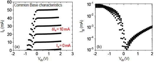
Figure 2: (a) Common base characteristics of III-nitride HET. (b) Base current vs collector voltage during common base measurement.
For positive VCB the base current is limited to an extremely low value of 10μA. The fact that the base current remains low is taken as an indication of near-ballistic transport from emitter to collector. Significant scattering would drop the electrons in the base to the Fermi level, below the base–collector barrier, increasing the base current.
Some preliminary spectroscopic measurements were also made using the device that showed peaks of Maxwellian shape in conductance measurements that reflect the electron energy distribution at the base–emitter interface.
The lead author of the paper, Sansaptak Dasgupta, comments: “From conductance measurements, we find that the distribution remains similar after the electrons cross the base and get collected at the collector. This is a signature of the near-ballistic transport. However exactly how many electrons are ballistic depends critically on matching the injection energy (VEB) with the collection energy
(VCB). That is tough for these devices, where the emitter series resistance was high. In subsequent devices, we have lowered the emitter contact and series resistances, and thus can get a true indication of VEB as we inject the electrons. However, that would be the subject of a different paper.”
The researchers also report that they have also produced devices with higher B–C barriers to reduce leakage currents, enabling efficient common emitter operation that will be reported on in the future.
The work was partially funded by the US Office of Naval Research (ONR).
AlGaN/GaN/AlGaN GaN templates Lumilog MBE
The author Mike Cooke is a freelance technology journalist who has worked in the semiconductor and advanced technology sectors since 1997.