- News
21 June 2011
Combining high current with high transconductance
France’s Institute of Electronic, Microelectronic and Nanotechnology (IEMN) has given a new report of record performance for nitride semiconductor high-electron-mobility transistors (HEMTs) on silicon [Farid Medjdoub et al, Appl. Phys. Express, vol4, p064106, 2011]. The latest results give high current (more than 2A/mm) and transconductance (~600mS/mm) figures for the structure, along with improved frequency characteristics. The DC performance is described as being “well beyond the highest reported values of any GaN-on-Si HEMTs”.
The devices use a novel aluminum nitride (AlN) barrier structure that the group has reported on in the past month in two other journal articles (reported at AlN barrier increases output current from GaN/Si HEMTs and Record transconductance for nitride HEMT on silicon).
The use of AlN allows the barrier layer to be much thinner than normal (less than 10nm), bringing the gate much closer to the channel region provided by the two-dimensional electron gas (2DEG) that forms at the interface with the gallium nitride (GaN) buffer layer. Conventional barriers consist of AlGaN, while some groups are developing indium aluminum nitride (InAlN) as an alternative.
The thinner AlN barrier allows smaller HEMTs to be developed, increasing frequency performance. The IEMN researchers are seeking to extend the frequency for “the next generation of millimeter-wave (mmW) power amplifiers”.
Other desirable potential features, besides high frequency, are high breakdown voltage, high current density and low cost. The use of a silicon substrate is aimed at the last feature, giving the potential for widespread adoption of nitride transistor technology if the growth challenge of large lattice mismatch between the materials can be overcome.
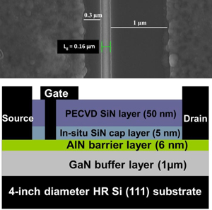 IMEC spin-off EpiGaN in Leuven, Belgium was commissioned to grow all the epitaxial material on 4-inch (100mm)-diameter (111)-oriented silicon wafers using metal-organic chemical vapor deposition (MOCVD). The epitaxial structure included a 5nm in-situ silicon nitride (SiN) layer that was designed to relax the high tensile stress in the 6nm AlN due to the large lattice mismatch with the underlying 1μm GaN buffer (Figure 1).
Figure 1: Cross section of the fabricated AlN/GaN-on-Si HEMTs and SEM top view of the device after gate opening.
The structure is the same as used in the previous work (AlN barrier increases output current from GaN/Si HEMTs). Corresponding author Dr Farid Medjdoub credited the better results of the latest work on “process improvement”. The other work (Record transconductance for nitride HEMT on silicon) used a thinner 3nm barrier.
The gate length of the new device was smaller than before at 0.16μm, with gate–source and gate–drain distances of 0.3μm and 1μm, respectively. The previous devices had gate lengths of 0.2μm and gate–source and gate–drain distances of 0.4μm and 1.3μm, respectively. The device width was kept at 50μm. Device isolation was achieved using nitrogen implantation (instead of helium).
The maximum DC output current density for the new device was 2.3A/mm, “reflecting the high sheet carrier density provided by the AlN material that possesses the highest spontaneous polarization among all III–nitrides”. Room-temperature Hall measurement of the epitaxial material used to create the HEMTs gave an electron sheet concentration of 2.15x10¹³/cm2.
Under reverse bias of a Schottky diode, where the current should be small, the gate leakage was found to be less than 100μA/mm up to 80V. Buffer leakage, determined using a separate structure with two isolated ohmic contacts having 5μm spacing on the material, was less than 4μA/mm up to 200V reverse bias.
The researchers believe the in-situ SiN layer enhances the surface robustness of the high-quality AlN barrier, avoiding gate tunneling under high electric field.
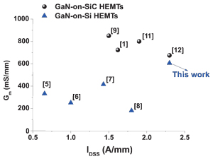 The extrinsic transconductance has a peak value of 606mS/mm at –1.6V gate potential and source–drain bias of 4V. The transconductance is more than 500mS/mm for VDS in the 2–6V range under the same gate potential. This performance puts the device into comparison with GaN HEMTs on expensive silicon carbide substrates that benefit from smaller lattice mismatch (and hence better crystal quality, giving an improved 2DEG) and high thermal conductivity (Figure 2).
Figure 2: Benchmarking of extrinsic transconductance as function of maximum saturated current density (IDSS) of GaN-on-Si HEMTs (blue triangles) and GaN-on-SiC HEMTs (black circles).
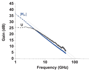 Frequency performance measurements were also carried out (Figure 3), giving extrinsic cut-off (fT) and maximum oscillation (fMAX) frequencies of 85GHz and 103GHz, respectively. These are high figures, given the “relatively high access resistances and residual losses most probably located at the buffer/Si substrate interface”. The high lattice mismatch between the buffer and silicon substrate is blamed for a 0.7dB/mm loss at 50GHz in coplanar waveguide measurements.
Figure 3: RF performance of 0.16μm x 50μm AlN/GaN HEMT on highly resistive silicon substrate. Extrapolation at –20 dB/dec yields fT of 85GHz and fMAX of 103GHz at VDS 4V and VGS –1.6V.
The cut-off gate-length product (fT x Lg) of 13.6GHz-μm suggests that downscaling the gate length “will allow very high-frequency operation considering the high aspect ratio achievable with sub-100 nm gate lengths.”
The previous 0.2μm device (AlN barrier increases output current from GaN/Si HEMTs) had a cut-off gate-length product of 10.4GHz-μm with an fT of 52GHz. The previous fMAX was 102GHz.
The researchers conclude: “The high-frequency performance achieved for a gate length of 0.16μm promises breakthrough millimeter-wave low-noise and high-power monolithically integrated amplifiers in a cost-effective way.”
Record transconductance for nitride HEMT on silicon
AlN barrier increases output current from GaN/Si HEMTs
The author Mike Cooke is a freelance technology journalist who has worked in the semiconductor and advanced technology sectors since 1997.