- News
29 June 2011
Protecting nitride LEDs from reverse bias ESD
Korean researchers have developed indium gallium nitride (InGaN) semiconductor light-emitting diodes (LEDs) with integrated shunt diodes to improve handling of reverse-bias electrostatic discharge (ESD) events up to 3kV [Sang-Mook Kim et al, Appl. Phys. Express, vol4, p072102, 2011]. The researchers from Korea Photonics Technology Institute (KOPTI) and Gwangju Institute of Science and Technology claim: “This LED is superior not only in terms of its ease of fabrication, but also in its high reliability.”
The researchers were seeking to improve the negative-bias ESD performance that at present is around 100V–1kV. Positive-bias ESD resilience tends to fall in the higher range of 1–3kV. Such devices are used in traffic signaling, large-scale displays and backlighting of liquid-crystal displays.
The difference in behavior for forward and reverse bias is attributed to high dislocation densities in the epitaxial material that it is used and in the lateral device structure needed for standard nitride LEDs that are grown on insulating sapphire substrates. These two adverse features allow large negative ESD voltage pulses to damage the LED.
A number of techniques have been used to protect devices against such damage — reducing defect density, external diodes, etc. However, these techniques are difficult to incorporate into manufacturing at low cost.
The KOPTI/Gwangju researchers used conventional In0.15Ga0.85N/GaN MQW 450nm (blue) LED structures grown on c-plane sapphire through metal-organic chemical vapor deposition (MOCVD). The LEDs were defined using photolithography and inductively couple plasma (ICP) etch down to the n-type layer. Indium tin oxide (ITO) was used as a transparent conductive ohmic electrode. The bond pads consisted of chromium-nickel-gold.
The researchers integrated shunt diodes into the LED to protect from ESD by extending the contact of the n-electrodes into the p-region (Figure 1). The Schottky barrier between the n-electrode and p-GaN was raised using an oxygen plasma treatment, designed to reduce reverse leakage during a negative-bias ESD event. Large leakage currents tend to damage the n-electrode and hence reduce device performance.
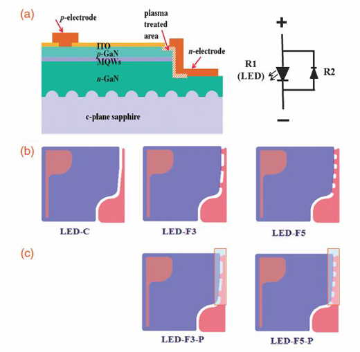
Figure 1: (a) Cross-sectional view and schematic circuit diagram showing an LED with an extended n-electrode, and top views of (b) conventional (LED-C), 3- (LED-F3) and 5- (LED-F5) finger n-electrode without, and (c) with plasma treatment (LED-F3-P and LED-F5-P). The shaded region of (c) indicates the plasma-treated area.
A further expected effect of oxygen plasma is to create nitrogen vacancies in the p-GaN, resulting in a pseudo-pn junction for the shunt diode.
An ICP power of 70W increased the contact resistance of the n-electrode to 56.1x10⁻³\Ohm-cm2, as determined by circular transmission-line structures on plasma-treated p-GaN surfaces. Lower ICP powers resulted in lower contact resistance.
Another technique to reduce the leakage current was to reduce the area of contact between the n-electrode using 3 fingers, rather than 5. This had the effect of reducing the contact area from 300μm2 to 180μm2.
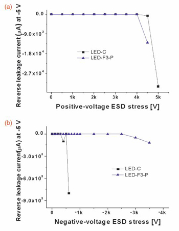 Commercial LEDs have a maximum reverse leakage specification of 50μA at –5V; the LEDs with 3-finger plasma-treated shunt diode had leakage currents in the range 0.02–21μA, meeting the requirement. The researchers believe they could further reduce the leakage under both reverse and forward bias by optimizing the plasma treatment and finger contact area.
Figure 2: (a) Positive- and (b) negative-voltage ESD characteristics of LED-C and LED-F3-P.
The ESD characterization was carried out with an ESS-606A (Noiseken) ESD tester that produces pulses according to the human body model. After each test, the leakage performance at –5V was measured and, if a 30% variation from the original performance was found, the device ‘failed’ (Figure 2). While the conventional diode failed under negative-bias ESD in the range 300–500V, the plasma-treated device with extended 3-finger n-electrode only failed at 3kV. The positive bias results are deemed by the researchers to be “not distinguishable”.
InGaN LEDs Reverse-bias electrostatic discharge
The author Mike Cooke is a freelance technology journalist who has worked in the semiconductor and advanced technology sectors since 1997.