- News
4 June 2011
High-brightness nitride LEDs on silicon through wafer bonding
Researchers based in Korea have used wafer bonding to create high-brightness LEDs from nitride on silicon material with 9.5mW light output power at an injection current of 20mA [Seung-Jae Lee et al, Appl. Phys. Express, vol4, p066501, 2011]. The work involved researchers from Korea Photonics Technology Institute and one researcher from Chonbuk National University.
The big attraction of silicon-based technology is the potential for lower costs, in terms of substrate prices, processing with standard tools, and the use of larger-diameter wafers (up to 300mm) for mass production/economies of scale.
Nitride semiconductors can be grown on silicon (Si) substrates oriented in the (111) crystal direction, but there is a large lattice mismatch, and different thermal expansion properties can introduce a large tensile stress, and even cracking, in the nitride layers. Also, because the bandgap of silicon is narrower than that of light emitted from nitride devices, there is heavy absorption of radiation that travels through the substrate material.
The basic epitaxial material for the Korean device was grown using metal-organic chemical vapor deposition (MOCVD) on n-Si(111) wafers. The active region consisted of five quantum wells of InGaN separated by GaN barriers. Before the active region, an AlN complex buffer and then Si-doped n-GaN layers were grown. The device layers were completed with a magnesium-doped p-GaN layer.
To overcome the problem of light absorption by the Si substrate, these LED layers with a reflecting layer deposited on top were transferred using wafer bonding techniques to another Si wafer (Figure 1). The ohmic p-GaN contact consisted of 200nm indium tin oxide (ITO), annealed at 650°C for one minute. The reflection metal was 200nm gold-copper alloy and the bonding metal was a series of gold-tin layers. A barrier of nickel-titanium-platinum layers was used to prevent damage of the reflecting by the bonding layers.
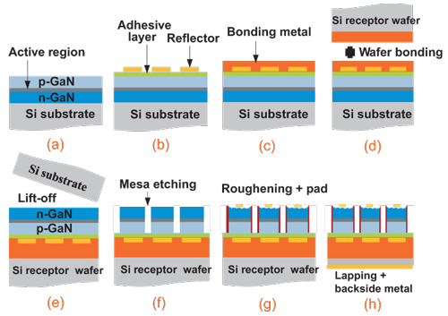
Figure 1: Fabrication process for vertical LED: (a) GaN-based LED grown on Si(111) substrate, (b) ITO and reflection metal deposition, (c) barrier/bonding metal deposition, (d) wafer bonding to Si(100) receptor substrate, (e) removing Si(111) substrate, (f) mesa etching, (g) n-GaN roughening and formation of n-electrode, and (h) p-contact metallization after thinning Si.
 The p-Si(100) receptor wafer was prepared with a titanium-gold layer. The receptor and the LED wafers were bonded using a pressure of 4kg-f/cm2 for 30 minutes at 300°C. The material from the original n-Si(111) wafer was removed by lapping down to less than 50μm and then etching with xenon fluoride plasma.
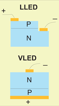
Figure 2: Lateral (LLED) and vertical (VLED) LED structures.
The LED device mesas were formed using inductively coupled plasma (ICP) etching. The sidewalls of the mesas were passivated with silicon nitride and then the n-GaN surface was roughened using a boiling potassium hydroxide solution. The p-Si(100) material was thinned to 100μm by lapping and then the backside titanium-gold metal was deposited.
The epitaxial material was used to create vertical (VLED) and lateral (LLED) LED structures (Figure 2). The LLED configuration is the one that has to be used when the epitaxial material is deposited on insulating substrates. However, where both surfaces of the LED material are conducting, the VLED structure can offer better performance through more even distribution of the current flow.
The tested chips had an area of 300μm x 300μm. One effect of the vertical structure was to slightly reduce the series resistance so that the operating voltage of 3.2V at 20mA injection current was comparable to that of sapphire-based devices. The LLED voltage at 20mA was 3.5V. At the same injection current, the VLED emitted 9.2mW of light output, more than 2.6x that of the LLED’s 3.5mW performance (Figure 3).
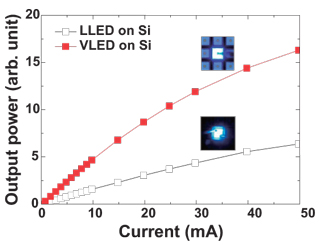 The researchers comment: “The superior light emission from the VLED can be attributed to the relatively larger effective light-emitting area by using only one electrode, the providing of better reflection of the downward-absorbing light by the reflection metal layer, and improvement of the light-extraction efficiency by roughening the n-GaN surface. Furthermore, the current can spread uniformly without an n-metal layer or a transparent layer (ITO), because the VLED structure was p-side down and n-side up, with an n-metal electrode. Accordingly, the VLEDs do not exhibit the current-crowding problem on the top emission area.”
Figure 3: Comparison of the light output power vs current (L–I) characteristics of VLED and LLED.
The researchers also tested shifts in wavelength as the injection current increased. In the low-current region there was a blue-shift, meaning that the produced photons had higher energy and shorter wavelength. Such behavior is often seen as carrier densities increase because filling with electrons and holes widens the separation in the respective energy levels. At higher currents, self-heating effects begin to affect the energy-level structure itself and the bandgap becomes narrower, leading to lower-energy photons and longer-wavelength emissions (red-shift).
Both devices began emitting light with wavelengths around 454nm. The VLED emission wavelength red-shifted down to around 452.5nm at about 41mA, and then increased to about 453.5 at 100mA. The LLED red-shifted much further to around 450.5nm at 60mA, afterwards increasing to ~451.7nm at 100mA.
The researchers believe that, by detaching the VLED from the Si(111) substrate, the tensile strain in the structure was much reduced. In the LLED, such tensile strain leads to piezoelectric polarization electric fields that affect the device performance. Such fields tend to make it harder for electrons and holes to recombine to produce photons, a behavior that is called the quantum-confined Stark effect (QCSE). The QCSE reduces recombination efficiency and also increases wavelength shifts.
The researchers conclude: “These results show the promise of Si as a large-area, inexpensive substrate for high-efficiency GaN-based LEDs with similar performance to devices on sapphire. It is expected that GaN-on-Si-based VLED technology will be very favorable for the applications of high-power and cost-effective solid-state lighting.”
Wafer bonding HB-LEDs GaN-on-Si MOCVD
The author Mike Cooke is a freelance technology journalist who has worked in the semiconductor and advanced technology sectors since 1997.