- News
3 March 2011
Lateral conduction, substrate-free deep UV nitride semiconductor LEDs
Nitek Inc and University of South Carolina (USC) have reported the first successful fabrication and characterization of lateral conduction, substrate-free aluminum gallium nitride (AlGaN) deep ultraviolet (DUV) LEDs grown on thick-AlN/sapphire templates [Seongmo Hwang et al, Appl. Phys. Express, vol4, p032102, 2011].
LEDs emitting in the deep ultraviolet (DUV, wavelengths <300nm) are being widely developed for air/water/surface/food purification/sterilization. Short wavelengths disrupt DNA molecules, killing microbiological organisms. Other possible applications include biomedical instrumentation and polymer curing.
Researchers are seeking to replace fragile, poisonous mercury lamps with a robust, safe alternative. Presently, the wall-plug efficiencies of DUV LEDs are at best about 2%, and operating lifetimes are only 1000hr at 20mA pump current. Being a first demonstration of a new technique, the Nitek/USC device falls short of the wall-plug efficiency of the best devices by an order of magnitude. Operation lifetime is not reported.
The Nitek/USC researchers began with grooved (0001) sapphire substrates on which an AlN layer was grown using metal-organic chemical vapor deposition (MOCVD). The AlN layer was deposited using maskless pulsed-lateral overgrowth (PLOG) to reduce threading dislocation densities (particularly in the ‘wings’). Another effect of the PLOG material was reduced thermal impedance. Apart from improved material quality in the subsequent epitaxial layers, the reduction in dislocations and thermal impedance also determine long-term lifetime reliability of devices. X-ray diffraction analysis gave the (102) ω-scan rocking curve a full-width at half maximum (FWHM) of 377arcsec.
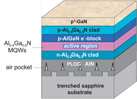 The epitaxial layers were grown using a combination of pulsed atomic layer epitaxy and low-pressure MOCVD. The LEDs (Figure 1) consisted of an active region with Al0.4Ga0.6N multi-quantum wells with Al0.6Ga0.4N barriers. The cladding layers consisted of Al0.5Ga0.5N.
Figure 1: Schematic of epitaxial structure of Nitek/USC 276nm LED.
An electron-blocking layer of p-AlGaN was included to reduce overshoot and recombination in the p-type GaN layer. Unfortunately there is no good way to produce thick p-AlGaN with high hole densities, so p-GaN is used for the p-contact. However, the p-GaN layer tends to absorb ultraviolet light. This is the main reason that flip-chip mounting is used for UV LEDs where the chip is turned over and the last-grown p-GaN layer is bonded to the submount.
The resulting epitaxial structure was formed into 100μm square shaped mesas using lithography and reactive-ion chlorine etching through to the n-type AlGaN layer. The n-contact consisted of ohmic titanium-aluminum-nickel-gold layers. These metals were then annealed at 950°C. The nickel-gold p-contact was annealed at 550°C.
A lateral-conduction scheme is used with the contact pads on the same side of the LED chip. Although lateral conduction has disadvantages in terms of current bunching effects, it has the advantage of clearing the emission surface of contact pad obstructions, as needed for vertical conduction (contact pads on top and bottom of chip).
The LEDs were diced into 2x2 arrays and flipped on silicon carbide submounts and bonded with gold-tin solder bumps. The sapphire was removed by separation and lift-off using high-energy excimer laser pulses directed through the substrate. Electrical measurements before and after the lift-off showed no noticeable change in behavior. This means that the potential for damage of the laser process had been avoided. The resulting substrate-free flip-chip LED array was then bonded into a transistor outline package header (TO-39).
The turn-on voltage of the device was 6V. Unfortunately, the resistances of the device were higher than expected: the series resistance was about 90Ω, and both contact resistances were more than one order of magnitude higher than the researchers’ typical values. The group comments: “These results are indicative of the need to systematically optimize the doping parameters for LED structures grown on PLOG-AlN templates.”
In terms of emission spectrum, there was a main wavelength of 276nm (full-width half-maximum 12.4nm), along with a broader parasitic radiation band around 410nm (violet, photon energy ~3.02eV). The main peak was around 250x higher than that of the broad parasitic emission.
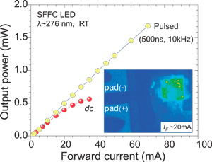 Light output power (Figure 2) of one 100μm square devices was measured in both pulsed (0.5% duty cycle) and direct current operation using an integrating sphere and calibrated silicon detector. In direct current mode, the output power was limited to less than 0.6mW (reached at 30mA current, 0.4mW @ 20mA, a quick calculation from graphs in the paper give a wall-plug efficiency of about 0.4mW/20mA/8V = 0.25%).
Figure 2: Light output power vs pump current (L–I) characteristics of a 100μm x 100μm substrate-free flip-chip single LED measured under direct current and pulsed operation. Inset: plan-view CCD image of LED biased at 20mA forward current.
Pulsed operation, avoiding self-heating effects, enabled an output power of 1.7mW at 70mA. The self-heating seen in direct-current mode was particularly strong due to the high-resistance problem mentioned above. This would also impact wall-plug efficiency.
The researchers report that some improvement has been seen in light extraction through thinning the exposed surface of the LEDs. They attribute the improvement to the reduction of light scattering from the air pockets of the PLOG AlN process. The researchers also believe that dramatic increases in output power would result from “eliminating the light scattering mechanisms together with the implementation of backside roughening and the collection of waveguided light”. Such techniques have been successful in enhancing the performance of visible LEDs (e.g. a 50% boost from surface texturing). The ‘waveguided light’ effect refers to light transmitted along the planes of the epilayers and emitted at the edge of the device.
The author Mike Cooke is a freelance technology journalist who has worked in the semiconductor and advanced technology sectors since 1997.
Join Semiconductor Today's LinkedIn networking and discussion group