- News
11 March 2011
InGaAs tunnel FET with ON current increased by 61%
University of Texas at Austin researchers have developed indium gallium arsenide (InGaAs) tunneling field-effect transistors (TFETs) with ON current increased by up to 61% [Han Zhao et al, Appl. Phys. Lett., vol98, p093501, 2011]. This was achieved by changing the tunnel junction layers, consisting of heavily p-type and intrinsic material (p++/i), to heavily p-type and n-type (p++/n+).
The effect of using an n-type layer in the tunneling diode is to reduce the tunneling width and increase the tunneling field, which in turn should allow for increased ON currents and better subthreshold behavior.
Logic transistors need a high ON current and low OFF current to operate effectively. This becomes difficult when the threshold voltage is low, and particularly so for devices with large subthreshold swing (SS). Low threshold voltages are desired to reduce power consumption and heat generation.
Theoretical work suggests that inter-band tunneling field-effect transistors (TFETs) are not subject to the SS limitation of 60mV/dec at room temperature for conventional MOSFETs. Application of these ideas in silicon or germanium has resulted in devices with low ON current, resulting from the high tunneling barrier.
Recently InGaAs has been proposed as a channel material for high-performance, high-density logic, due to its much higher mobility value. InGaAs tunneling structures might allow higher ON currents due to a low carrier effective mass and narrow bandgap.
Pennsylvania State University with Cornell University demonstrated the first InGaAs TFETs in 2009, but the saturation/ON current was low (20μA/μm) and the SS was more than 150mV/dec. Texas-Austin managed to double the ON current and reduce SS to 96mV/dec last year (2010). These results have to be compared with 65nm strained silicon technology that has achieved ON currents of 1.62mA/μm (1620μA/μm) with SSs of 105mV/dec.
The latest Texas-Austin TFETs have a vertical structure, using molecular-beam epitaxial layers to form the different regions needed to make the channel and tunnel injector (Figure 1). Conventional CMOS manufacturing tends to favor lateral/planar structures.
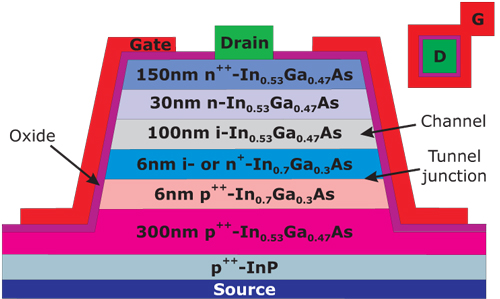
Figure 1: Cross section and top view (inset) of ring-type In0.7Ga0.3As TFETs using p++/i or p++/n+ tunneling junctions with HfO2 gate oxide and TaN gate electrode.
The tunnel junction consisted of either a p++/i (undoped) or p++/n+ junction of In0.7Ga0.3As. The p-type material was achieved using beryllium (Be, 2x10¹⁹/cm3) and the n-type using silicon (Si, 2x10¹⁸/cm3) doping. The doping in the n-type layer must be low enough to ensure that it is fully depleted by the p++ layer. Without the depletion, the injection mechanism into the undoped channel layer would be thermionic emission, as in conventional MOSFETs.
The etching to create the ‘ring-type’ TFET used a citric acid/hydrogen peroxide solution in water. The etch stopped about 100nm into the 300nm p++-In0.53Ga0.47As layer (leaving 200nm). The gate insulator consisted of 5nm of hafnium dioxide (equivalent to a silicon dioxide thickness of 1.2nm) applied using atomic layer deposition at 200°C. The gate electrode was sputtered tantalum nitride.
The drain contact consisted of gold-germanium/nickel/gold and the source was a back contact of chromium and gold; both contacts were applied with electron-beam evaporation. The wafer was then annealed at 300°C in nitrogen to create ohmic source/drain contact behavior.
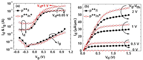
Figure 2: (a) Drain current (Id-Vg) and gate current (Ig-Vg) vs gate voltage characteristics of In0.7Ga0.3As TFETs using p++/i or p++/n+ tunneling junctions and 5nm HfO2 gate oxide. (b) Drain current–voltage (Id–Vd) curves at different gate voltages over threshold (Vg–Vth) for the same devices (gate width 560μm, gate length 100nm).
The minimum subthreshold swing was 84mV/dec at a drain bias of 0.05V for both types of tunneling junction. The similarity of the SS for these devices is thought to result from two competing factors: the shorter tunneling width for p++/n+ tunneling junctions reduces SS relative to p++/i tunneling; and, higher doping concentration in the n+ layer gives weaker coupling between semiconductor and gate in the MOS structure, increasing SS.
The SS was higher than 60mV/dec, the researchers believe, due to a poor III-V/oxide interface and, possibly, dopant diffusion in the tunneling junction (as shown in secondary-ion mass spectroscopy analysis). The interface trap density at the III-V/oxide interface was estimated to be ~4x10¹²/eV/cm2.
Gate leakage was less than 0.2mA/cm2 at gate voltage of 1V. The threshold voltages of the p++/i and p++/n+ tunnel junction devices were 0.21V and 0.15V, respectively. The drive current of the p++/n+ device was enhanced above that of the intrinsic device by 61% and 20% at 0.5V and 2V gate voltage over threshold, respectively. The 2V p++/n+ drive current was 60μA/μm.
The researchers comment: “This improvement is believed to be due to a shorter tunneling width and a higher tunneling electric field for TFETs using p++/n+ tunneling junctions.”
The researchers carried out simulation using Sentaurus Device @ Synopsis software to find the performance trends for varied n+ doping of the tunnel junction. The simulations suggested that an n+ doping of 8x10¹⁸/cm3 might be optimum: above this, the off-current is too high; below this and the on-current degrades. Since the simulation was not calibrated, the researchers stress that this result is only a guideline, and hence suggestive that optimization in actual devices could lead to improved performance.
Funding came from Intel Corp, the Texas Advanced Research Program, the US National Science Foundation Integrative Graduate Education and Research Traineeship (NSF IGERT) program, SEMATECH, and Micron Foundation.
The author Mike Cooke is a freelance technology journalist who has worked in the semiconductor and advanced technology sectors since 1997.
Join Semiconductor Today's LinkedIn networking and discussion group