- News
5 May 2011
UCSB reports N-polar HEMT power density record
A University of California Santa Barbara (UCSB) research team has achieved a new record for output power density of N-polar aluminum gallium nitride/gallium nitride (AlGaN/GaN) high-electron-mobility transistors (HEMTs) [Seshadri Kolluri et al, IEEE Electron Device Letters, vol32, p635, published online 15 April 2011].
The headline performance figure for the device was 12.1W/mm output power density at 4GHz operation and 50V drain bias (Table 1). The researchers comment: “To the best of our knowledge, the device reported in this letter showed the highest output power density for an N-polar GaN HEMT, and also matched the highest output power density for a Ga-polar device grown on a sapphire substrate”.
Device |
Substrate |
VDS |
POut |
PAE |
(V) |
(W/mm) |
(%) |
||
MOCVD N-face |
Sapphire |
50 |
12.1 |
55 |
MBE N-face |
SiC |
40 |
8.1 |
54 |
MOCVD Ga-face |
Sapphire |
50 |
12 |
58 |
SiC |
135 |
41.6 |
60 |
|
MBE Ga-face |
SiC |
42 |
13.7 |
55 |
Table 1: Comparison of 4GHz large-signal performance of different GaN HEMTs. All results from UCSB work, except for Cree Santa Barbara Technology Center (MOCVD Ga-face on SiC substrate). The latest UCSB work is MOCVD N-face/sapphire.
However, the researchers note that Ga-polar AlGaN/GaN HEMTs grown on SiC presently show significantly better output power density (more than 40W/mm). These Ga-polar HEMTs, developed by Cree Santa Barbara Technology Center, used multiple field plates to massage the electric field distribution in the device layers. The use of SiC allows much better heat dissipation since it has a much higher thermal conductivity than sapphire. Devices with Ga-polar AlGaN/GaN structures are seen as having much potential for power amplification of microwave frequencies ranging from L-band (40–60GHz) to W-band (75–110GHz).
Advantages of reversing the polarity of the nitride semiconductor layers to being N-polar include lower contact resistance. “Development of N-polar MOCVD HEMTs on SiC substrates is expected to reduce the limitations due to self-heating and improve the large-signal performance of the devices significantly,” the researchers add. Much of the work in this direction has been carried out at UCSB.
The researchers put particular stress on their use in the new devices of silicon nitride passivation and recessed gate structures with integrated slant field plates “to prevent dc to RF dispersion and improve the breakdown voltage”. Further features include reduced source-to-drain spacing (reduced parasitic resistance) and increased output bias voltage.
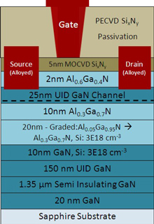 The structure (Figure 1) was grown using metal-organic chemical vapor deposition (MOCVD) with trimethyl-gallium/aluminum (TMGa/TMAl) and ammonia as precursors on (0001) sapphire mis-oriented 4° toward the a-sapphire-plane. The researchers comment: “Growth on a misoriented substrate was essential to achieve smooth, high-quality N-polar films”.
The N-polar film was initiated by exposing the sapphire surface to ammonia at high temperature. The semi-insulating GaN layer was achieved through iron-doping using bis-cyclopentadienyl-iron ((Cp)2Fe).
Ohmic source–drain contacts consisted of titanium/aluminium/nickel/gold (Ti/Al/Ni/Au) annealed at 870°C in nitrogen. These electrodes reached through the cap layers, making contact with the GaN channel layer. A boron trichloride/chlorine reactive ion etch (RIE) created the transistor mesa structure, which was then passivated with silicon nitride applied using plasma-enhanced CVD (PECVD).
A timed gate recess etch was performed using carbon tetrafluoride/oxygen plasma. The gate metal structure was nickel/gold/nickel (Ni/Au/Ni). The nominal gate length was 0.7μm with a gate–drain spacing of 0.8μm. The gate width was 2μm x 50μm.
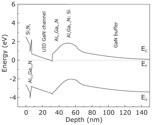
Figure 1: a. (above) Schematic cross section, and b. (below) simulated band diagram of device.
The channel direction was aligned with the direction of the growth steps that result from use of the mis-cut sapphire substrate. The reason for this is that that conductivity was found to be greatest in this direction in Hall-effect measurements on the epitaxial material.
Further performance specifications include cut-off (fT) and maximum oscillation (fMAX) frequencies of 16GHz and 40GHz, respectively, at a drain bias of 17V. The three-terminal breakdown voltage (leakage current 1mA/mm) with gate biased at pinch-off was found to be in excess of 170V.
The UCSB work is supported in part by the US Office of Naval Research (ONR) Millimeter-wave Initiative for Nitride Electronics (MINE) project.
N-polar AlGaN/GaN HEMTs Sapphire substrates MOCVD SiC substrates
The author Mike Cooke is a freelance technology journalist who has worked in the semiconductor and advanced technology sectors since 1997.