- News
11 November 2011
Two steps to high breakdown voltage in GaN diodes
Researchers at Hosei University and Hitachi Cable Ltd have increased the breakdown voltage (VB) for gallium nitride (GaN) semiconductor p-n junction diodes to more than 1100V and reduced the leakage current to the nanoampere range [Yoshitomo Hatakeyama et al, IEEE Electron Device Letters, published online 13 October 2011]. This performance was achieved with a new two-step process for creating the p-electrode (anode) with a field plate that avoids plasma damage of the p-nitride semiconductor surface.
The on-resistance (Ron) was also reduced to 0.4mΩ-cm2 for a 50μm diameter device, allowing a very high value for Baliga’s figure of merit (VB2/Ron) of 3.0GW/cm2. “These are the best values ever reported among those achieved by GaN p-n junction diodes on free-standing GaN substrates,” the researchers comment.
Field-plate structures are used in high-voltage components to create more uniform electric fields in semiconductor materials, reducing the field concentrating effects of sharp corners, for example, to avoid going beyond the critical electric field for the material. Gallium nitride has a large value for the critical breakdown field of ~2–3MV/cm at 300K. This is similar to the value for silicon carbide (SiC) (2.2MV/cm), but far exceeds that of silicon (0.3MV/cm). Gallium nitride also benefits from a higher electron mobility than SiC.
The Hosei/Hitachi devices were grown on free-standing GaN substrates to reduce defect densities that also impact breakdown performance and leakage. The diode nitride semiconductor growth was through metal-organic chemical vapor deposition (MOCVD) on these substrates. Low threading dislocation densities of ~106/cm2 were achieved by using substrates that were fabricated using the void-assisted separation method.
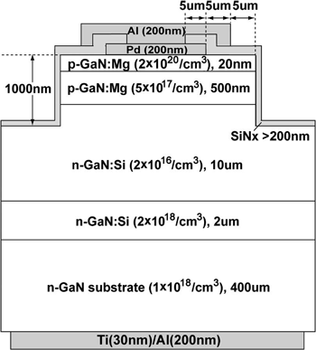 Figure 1: Schematic cross section of the GaN p-n junction diode with silicon nitride (SiNx) passivation and aluminum (Al) field-plate (FP) structure.
The gallium and nitrogen precursors were trimethyl-gallium (TMG) and ammonia (NH3), respectively. The silicon (n-type) and magnesium (p-type) doping were achieved through silane (SiH4) and bicyclopentadienyl-magnesium (Cp2Mg), respectively. After the growth of the epitaxial GaN layers (Figure 1), a thermal anneal was performed at 700°C to activate the Mg acceptors.
The researchers produced three sorts of device: devices with field plate and silicon nitride passivation (Figure 1), devices without field plate or passivation, and, devices with passivation but without field plate.
In making the field plates, the researchers were keen to avoid the damage that can result from plasma etching by using a two-step process.
First, the mesa structure was created using inductively coupled plasma etching. Circular palladium (Pd) electrodes formed an ohmic contact with the top p-GaN layer.
A 200nm silicon nitride film was then sputtered onto the whole chip. This avoided damage to the interface between the Pd and p-GaN. Contact holes were made in a wet-etch process (less damaging than dry plasma etch). The aluminum (Al) field plates were then deposited.
The titanium-aluminum (Ti/Al) electrode was then placed on the rear n-GaN surface. The metal structures (Pd, Al, Ti/Al) were created using electron-beam deposition.
Diodes with 50μm, 180μm and 780μm diameter were produced. These diodes had similar performance according to type. The devices with silicon nitride passivation and field plates continued to operate in reverse bias up to –1100V with leakage around 10-9A (1nA). Removing the field plates, but keeping the silicon nitride passivation, caused breakdown to occur at less than 650V; removing both factors reduced the breakdown further to less than 450V.
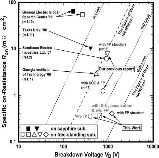
Figure 2: Relations between the specific ON-resistance and breakdown voltage for the fabricated GaN p-n and p-i-n junction diodes in this work and previously reported work. The dotted lines represent the theoretical Baliga figure of merit VB2/Ron for various values and material limits based on dielectric constant, electron mobility, and critical breakdown electric field, respectively (εxμxEc3).
The on-resistance was reduced from a value of 1.2Ω-cm2 for a 50μm diameter device with field plate previously reported by the same researchers to 0.4Ω-cm2 in the new work. The breakdown voltage of the previous device was 798V. The researchers compared their new values of on-resistance and breakdown voltage with those of other devices (Figure 2).
GaN GaN diodes GaN substrates MOCVD
The author Mike Cooke is a freelance technology journalist who has worked in the semiconductor and advanced technology sectors since 1997.