- News
14 November 2011
LayTec launches EpiTT 3W for simultaneous reflectance measurements of three wavelengths
LayTec AG of Berlin, Germany (which makes in-situ metrology systems for MOCVD processes) says that, in response to growing market demand, it is launching a new version of its EpiTT reflectometer that offers three simultaneous reflectance measurements. With EpiTT 3W, more complex in-situ growth studies of compound semiconductor devices composed of materials with rather wide band edges can now be performed.
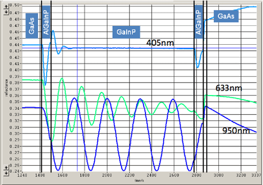
Graphic: Typical AlGaInP/GaInP double hetero-structure on GaAs grown for test purposes.
Tobias Roesener at Fraunhofer Institute for Solar Energy Systems (ISE) in Freiburg was one of the first customers to use the EpiTT 3W. He is working on III-V growth on silicon for future solar cell applications in an Aixtron CRIUS metal-organic chemical vapor deposition (MOCVD) system.
“The reflectance measurements at 633nm and 950nm have already been very helpful for us,” comments Roesener. “Now with the addition of the 405nm reflectance measurement in my case l got far more sensitive access to the surface morphology. Particularly, it allows me a much better monitoring of surface morphology evolution in thinner layers such as GaInP after only 50 to 100nm,” he adds. “The 633nm reflectance measurement is perfectly suited for GaInP growth control. At this wavelength we determine growth rates of layers which are below 100nm thick. The reflectance at 950nm is better suited for thicker layers.”
Roesener adds that, for growth of germanium layers, the application of the 950nm signal is extremely useful. For homo-epitaxial growth of germanium under different growth conditions (temperature, pressure, gas flows) the growth rate and the decomposition of the source materials can be derived in-situ in one single epitaxial process. “This saves me a lot of development time,” he states.
The EpiTT 3W is equipped with 405nmn, 633nm and 950nm reflectance as a standard and is hence suited to all III-As/P and III-nitride processes.
The new 3W option is also available for LayTec’s EpiCurve TT systems. All existing EpiTT, Twin TT and EpiCurve TT systems in the field can be upgraded on-site.
Sales engineers sought
LayTec plans to expand its international sales department and is looking for new sales engineers. Interested parties with a technical or scientific background in the field of semiconductor epitaxy, thin-film technologies or optical metrology can contact Walter Gibas (phone +49 (0)30 / 39 800 80-18 or e-mail walter.gibas@laytec.de). Relevant experience as a sales engineer is welcome.