- News
26 November 2011
Grading barriers for improved hole transport
Researchers based in Taiwan have used graded quantum barriers (GQBs) to reduce droop effects in nitride light-emitting diodes (LEDs) [C. H. Wang et al, Appl. Phys. Lett., vol99, p171106, 2011]. The drop in efficiency at 200A/cm2 from the peak values were 34% for a conventional LED, but only 6% for a device with GQB. The researchers were associated variously with National Chiao-Tung University (NCTU) and LED chip maker Epistar Co Ltd. These institutions reported earlier this year on graded electron-blocking layers [Good grades for reducing nitride LED efficiency droop].
Leading explanations for droop effects in nitride semiconductor devices include Auger recombination, electron overflow, hole transport barriers, and polarization fields. Auger recombination is a reduction in radiative recombination in favor of many-body interactions that can occur at higher carrier densities without light emission.
Electron overflow occurs where the electrons do not recombine with holes in the active region and reach the p-contact layers where they recombine non-radiatively. Hole transport problems arise because these quasi-particles are heavier and less mobile than ‘electrons’ in most semiconductors, including nitrides. Polarization effects arise from the more ionic nature of the III-nitrogen bond compared with group IV (e.g. silicon) semiconductors.
The GQB structures of the NCTU/Epistar work were designed to improve hole distribution through the active region. A number of other research groups have found that multi-quantum well (MQW) structures tend to emit light only from the last well before the p-contact region. This defeats the purpose of the MQW, which is to increase the volume of active material, hopefully increasing light output, while allowing the growth of strained indium gallium nitride (InGaN) wells that have a critical thickness of the order of nanometers before the quality degrades significantly.
Simulations were used to design the GQB so that the barrier to hole transport is reduced. The NCTU/Epistar structures were grown on c-plane sapphire using metal-organic chemical vapor deposition (MOCVD). The template layers consisted of nucleation layer of GaN grown at low temperature, followed by 4μm of n-GaN. On top of this, ten pairs of InGaN/GaN were used as a pre-strain layer. The active region consisted of six pairs of InGaN/GaN forming multi-quantum wells. The p-contact consisted of a 20nm 15%-Al p-AlGaN electron-blocking layer and 200nm of p-GaN.
The graded quantum barrier device had InGaN barriers, rather than pure GaN, which had graded In content from 5% to 0% along the c-direction, designed to counteract the effect of polarization electric fields. The grading was achieved through ramping the In/Ga ratio, to avoid changes in the growth rate that would result from temperature variation (another technique used for composition grading).
The fabricated LED chips had indium tin oxide (ITO) transparent conducting layers on the p-electrode and nickel-gold metal contacts. The typical chip sizes were 300μm x 300μm. At 22A/cm2 injection current density, the emission wavelength was ~450nm (blue).
The efficiencies (Figure 1) of the two devices compared well in terms of droop behavior with simulated values. The lower efficiency of the GQB device compared with the simulation is attributed to non-optimized epitaxial parameters for the graded composition barriers.
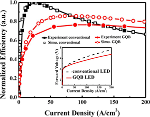 Figure 1: Experiment and simulation normalized efficiency for conventional and GQB LEDs. Inset: current–voltage (I–V) characteristics of conventional and GQB LEDs.
The series resistance was reduced in the GQB device at 6.5Ω, compared with the conventional device value of 8.2Ω. The reduction is reflected in the forward voltages at 22A/cm2 of 3.4V in the conventional LED and 3.27V in the GQB device.
Although the droop effect is reduced, the actual efficiency for the GQB LED at 20A/cm2 is only 70% that of the conventional device. Although at higher currents the GQB device does exceed that of the conventional device in efficiency, 20A/cm2 is a typical operating current for nitride LEDs (partly because of the droop problem). Such reduced efficiency is also seen in other droop reduction techniques.
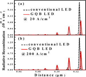 Figure 2: Calculated radiative recombination rates of conventional and GQB LEDs at current densities of (a) 20A/cm2 and (b) 200A/cm2.
Simulations suggest that the efficiency problem for the GQB device is creating a suitable overlap between the electron and hole distributions to maximize radiative recombination (Figure 2). The model shows a congregation of electrons and holes in the last well before the p-type layers for the conventional device, particularly at low currents. The GQB LED has higher hole concentration in the fifth rather than sixth well, but higher electron concentration in the sixth well (as for the conventional device), at 20A/cm2. The mismatch reduces efficiency.
At 200A/cm2, simulations give noticeable peaks for the individual electron and hole concentrations in all the wells for the GQB device (higher at the p-end), but only in the fifth and sixth wells for the conventional LED model.
The researchers conclude: “These results indicate that to reduce droop behavior without deteriorating the total recombination, one should pay more attention to the spatial distribution between holes and electrons”.
Good grades for reducing nitride LED efficiency droop
Varying wells to combat LED efficiency droop
National Chiao-Tung University Epistar LED efficiency droop GaN
The author Mike Cooke is a freelance technology journalist who has worked in the semiconductor and advanced technology sectors since 1997.