- News
29 November 2011
Non-polar laser diode power comparable to c-plane devices
University of California Santa Barbara and Japan’s Mitsubishi Chemical Corp have developed aluminum gallium nitride (AlGaN) cladding-free (ACF) m-plane nitride semiconductor laser diodes (LDs) with output powers comparable to state-of-the-art single-stripe emitter c-plane devices [R. M. Farrell et al, Appl. Phys. Lett., vol99, p171113, 2011].
There is much interest in non-polar or semi-polar nitride crystal orientations that can eliminate or alter/reduce the large polarization electric fields that arise in c-plane materials and gallium nitride (GaN) and indium gallium nitride (InGaN) that form the active visible light-emitting layers in nitride semiconductor devices. Altering these fields could allow better performance to be realized.
Cladding layers in laser diodes are used to confine the electromagnetic field, creating the conditions needed for stimulated emission. AlGaN is often used for this, but has a large lattice mismatch with the underlying InGaN/GaN structures and is therefore difficult to grow with sufficient quality (e.g. without cracking, and with low defect density, etc).
UCSB has been working on AlGaN-cladding-free technology since 2007. Its technique involves using separate-confinement heterostructures of InGaN or GaN and thicker InGaN quantum well regions.
Reducing the Al-content of cladding layers has allowed higher maximum output powers and reduced catastrophic optical mirror damage (COMD) to be realized in such devices. The COMD effect occurs because of high field densities at the mirror facets of the laser cavity. The AlGaN-cladding-free device expands the optical field distribution of the transverse mode. Also, such devices are more resistant to sudden failure or gradual degradation, offering the prospect of higher reliability and higher-power operation.
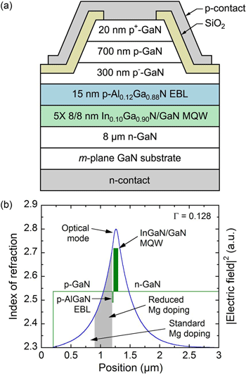 The epitaxial structures (Figure 1a) were grown using metal-organic chemical vapor deposition (MOCVD) on a nominally on-axis free-standing m-plane GaN substrate manufactured by Mitsubishi Chemical. The active region consisted of a five-period multi-quantum well (MQW) structure of InGaN with GaN barriers. The InGaN wells were 8nm thick, which is much thicker than the usual 2–3nm. Although the 15nm electron-blocking layer (EBL) contained p-AlGaN, the subsequent cladding layers did not. Simulations (Figure 1b) suggest that the UCSB structure should have a transverse confinement factor in the active region (Γact) of 0.128 at a lasing wavelength of 410nm (violet).
Figure 1: (a) Cross-sectional schematic of the device structure. (b) Calculated 1-D transverse mode profile.
The researchers designed the non-uniform doping of the p-GaN layers to decrease total absorption losses in the device by reducing phonon-assisted absorption by acceptor-bound holes. First-principles calculations have predicted that such losses should make the single largest contribution to modal loss in InGaN/GaN LDs and should scale with the density of the magnesium-doping that is used to give p-type conduction in nitride semiconductors. The transverse confinement in the low-doped p--GaN layer is given as 0.282.
Ridge LDs were produced using a self-aligned dry etch and insulator lift-off process. The 900nm-deep ridges were aligned with the c-direction of the nitride crystal. Dry etching was used to make the mirror facets. The p-contact was palladium/gold and the n-contact aluminum/gold.
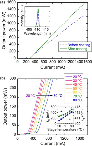 The resulting devices with 600μm-long, 10μm-wide ridges were subjected to pulsed currents with 2μsec pulse width and 1kHz repetition (Figure 2). Laser threshold currents were 244.9mA (4.08kA/cm2) before and 279.9mA (4.66kA/cm2) after facet coating. The threshold voltage of 7.7V for these devices is relatively high compared with state-of-the-art c-plane LDs. The researchers expect improvement with device optimization.
Figure 2: (a) Light output power vs current (L–I) characteristics collected before and after facet coating for a 600μm-long by 10μm-wide ridge waveguide LD. Inset: lasing spectra collected before and after facet coating. (b) L–I characteristics collected at varying stage temperatures. Inset: dependence of threshold current and lasing wavelength on stage temperature.
Although the facet coating increases the threshold current, it also increases the slope efficiency from 0.99W/A to 1.29W/A. The peak light output power also increased from 1.3W to 1.6W. The peak optical output power density at the front facet is estimated at 51.2MW/cm2 for the coated device. These levels are comparable to those that cause COMD in high-power c-plane InGaN/GaN LDs (40–70MW/cm2). Further, the level is higher than COMD levels reported for GaAs-based LDs under single-pulse excitation conditions (~30MW/cm2).
However, the new LDs were not limited by either thermal roll-over or COMD. The restriction came from the power supply used to drive the LD that was limited to currents less than 1.6A.
The spectra for at 600mA (before coating) and 700mA (after) show little shift in peak wavelength (Figure 2a inset). Thermal measurements (Figure 2b) of the threshold current resulted in a characteristic temperature of 95K, “comparable to the values reported for early c-plane LDs, but will need improvement for commercial applications,” according to the researchers. Similarly, the peak wavelength shift of 0.052nm/K was similar to early c-plane devices.
The UCSB/Mitsubishi work was supported by the Solid State Lighting and Energy Center (SSLEC) at UCSB and the US Defense Advanced Research Projects Agency (DARPA) VIGIL program.
The author Mike Cooke is a freelance technology journalist who has worked in the semiconductor and advanced technology sectors since 1997.