- News
19 October 2011
Ammonium sulfide vapor passivation for InGaAs
Researchers at European research center IMEC and Katholieke Universiteit Leuven (KULeuven) in Belgium have been investigating the possible use of ammonium sulfide ((NH4)2S) vapor (ASV) to passivate surfaces of indium phosphide (InP) and indium gallium arsenide (InGaAs) [Alireza Alian et al, Appl. Phys. Lett., vol99, p112114, 2011]. The researchers say that, based on their work, ASV treatment could be an efficient solution to the passivation of III-V surfaces.
The aim of the research is the attempt to use materials such as InGaAs as high-mobility channels in mainstream complementary metal oxide semiconductor (CMOS) circuits on silicon. At present, such work is impeded by the degradation in performance that occurs when dielectrics are applied as gate oxide insulation. Various new energy levels and charge traps are generated at oxide–semiconductor interfaces that impede transistor performance.
Ammonium sulfide treatment has been proposed as a way to reduce the generation of these interface states. Corresponding author Alireza Alian comments on the advantages of using vapour rather than solution: “One important advantage would be the elimination of the cleaning and drying steps after a wet solution treatment. The cleaning and drying steps are becoming more and more critical as the dimensions are shrinking. The other important advantage would be the cleaner processing; the ammonium sulfide solution is not available in a purity to be applied directly in a CMOS fab. The solution is usually full of all kind of metallic contaminations. You can assume that the contaminations are much less in density in the vapor than in the solution.”
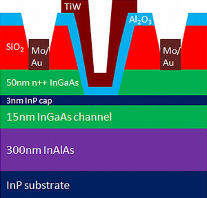 Test samples (Figure 1) were grown on (001) indium phosphide (InP) semi-insulating substrates using metal-organic chemical vapor deposition (MOCVD). Patterning was performed with a silicon dioxide hard mask. After mesa isolation etches, the gate recessing was performed using a selective wet etch of the highly doped n-type InGaAs layer down to the InP cap using a sulfuric acid/hydrogen peroxide solution in water.
Figure 1: Buried-channel transistor device structure. For the surface-channel device, the 3nm InP cap is removed during recess etch.
Buried- and surface-channel devices could be produced by either leaving the InP cap or etching through to the InGaAs channel with hydrochloric (HCl) acid solution. The buried-channel devices were treated with dilute HCl solution.
Some of the devices were treated further with ammonium sulfide vapor by holding the samples face down over a beaker containing ammonium sulfide solution for 3 minutes before immediate transfer to an atomic layer deposition (ALD) tool where the aluminum oxide (Al2O3) gate insulation was grown.
The 10nm gate oxide was deposited at 300°C. The gate metal consisted of 40nm of titanium-tungsten (TiW). Annealing was performed for 15 minutes in forming gas (10% hydrogen, 90% nitrogen) at 370°C.
Interface trap state densities (Dit) were assessed with capacitance–voltage measurements up to 1MHz on samples before gate oxide deposition (Table 1). Conductance measurements were also carried out at low temperature (77K) to probe Dit closer to the conduction band edge (70meV rather than 0.2eV for room-temperature measurement). While the room-temperature measurements suggest an increase in Dit for the ASV-treated samples, the low-temperature measurements give a lower value with a 30% (buried channel) or 40% (surface channel) reduction.
Type |
Surface treatment |
Dit 0.2eV below conduction band |
Dit 70meV below conduction band |
InGaAs surface channel |
HCl |
4x10¹²/cm2-eV |
2.5x10¹²/cm2-eV |
ASV |
7x10¹²/cm2-eV |
1.5x10¹²/cm2-eV |
|
InP capped channel |
HCl |
8x10¹²/cm2-eV |
7x10¹²/cm2-eV |
ASV |
9x10¹²/cm2-eV |
5x10¹²/cm2-eV |
Table 1: Interface trap density extracted from capacitance–voltage measurements.
In terms of transistor performance (Figure 2), the ASV indeed improves on-state current (1.5V overdrive voltage) and transconductance (0.1V drain voltage). The on-state current is increased by about a factor of 3. The researchers comment that their ASV process is “as efficient as the aqueous (NH4)2S in gaining a high drive current”.
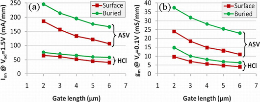
Figure 2: (a) Drive current (Ion) and (b) peak transconductance (gm) as functions of gate length for ASV- and HCl-treated surface-channel and buried-channel devices.
Despite the higher Dit in the midgap region, “as the nature of these states is donor-like, they will be electrically neutral during the ON-state operation of the device and will not influence the performance. The portion of the Dit located close to and above the surface Fermi-level position during the device operation is affecting the ON-state performance as these traps are electrically active.”
The researchers believe the effect of the higher Dit deeper into the bandgap may be seen in a poorer subthreshold slope behavior, particularly in the buried channel device, which may also suffer from surface doping effects caused by the ASV treatment of the InP cap. Such surface doping can increase depletion capacitance.
The researchers comment: “Comparing the buried-channel and the surface-channel devices, the doping effect seems insignificant on the In0.53Ga0.47As surface after ASV treatment, as the change in the subthreshold slope value is less prominent for the ASV-treated surface-channel device compared to the HCl treatment.”
The threshold voltage of the ASV-treated devices also shifted downward, more for the buried-channel device, due, it is thought, to “fixed charges formed at the interface of InP/Al2O3 resulting from the surface doping effect of ASV on the InP surface”. The researchers estimate a reduction in the oxide charge density after ASV treatment on the In0.53Ga0.47As surface of about 2.2x10¹⁸/cm3. Further, “The estimated fixed charge density as a result of the InP surface doping effect of ASV is about 1x10¹²/cm2 at the Al2O3/InP interface.”
X-ray photoelectron spectroscopy (XPS) examination of the indium 3d core levels suggested reduced concentrations of indium oxide in ASV-treated samples that were capped with 30 minute air exposure and 2nm Al2O3 from solid-source molecular beam epitaxy (SS-MBE) deposition.
The researchers comment: “These results indicate that indium or its oxides might be responsible for the drive current degradation. This can occur either due to the diffusion of In into the high-k layer creating border traps or the formation of interface states with an energy above the conduction band edge of In0.53Ga0.47As, which would degrade the carrier mobility.”
Financial support for the work came from the European Commission’s DualLogic project.
The author Mike Cooke is a freelance technology journalist who has worked in the semiconductor and advanced technology sectors since 1997.