- News
10 October 2011
Pyramid LED arrays on amorphous glass
Samsung Advanced Institute of Technology and Seoul National University have produced nitride semiconductor light-emitting diode (LED) structures on amorphous glass [Jun Hee Choi et al, Nature Photonics, published online 9 October 2011].
The structures consisted of an array of nearly single-crystalline truncated pyramids of gallium nitride (GaN) on which further layers of indium gallium nitride (InGaN) multi-quantum wells, magnesium-doped p-GaN, polymer filling and indium tin oxide (ITO) were deposited.
The researchers see potential applications as including using the pyramids as pixels in displays such as for large-area inorganic LED televisions, concluding: “This method should provide a new and attractive tool for realizing ideal high-performance electroluminescence devices that demonstrate both low cost and high device performance, as well as scalability to large sizes.”
The structures were begun with growth of the GaN pyramids on 2-inch fused silica glass wafers. The growth of nearly single-crystalline GaN on these wafers uses a ‘pre-orienting layer’ of thin-film titanium followed by a GaN nucleation layer (Figure 1a). The titanium is deposited in an evaporation process, and the GaN is deposited in low-temperature (560°C) metal-organic chemical vapor deposition (MOCVD) using a Sysnex system with trimethyl-gallium and ammonia sources in hydrogen carrier gas.
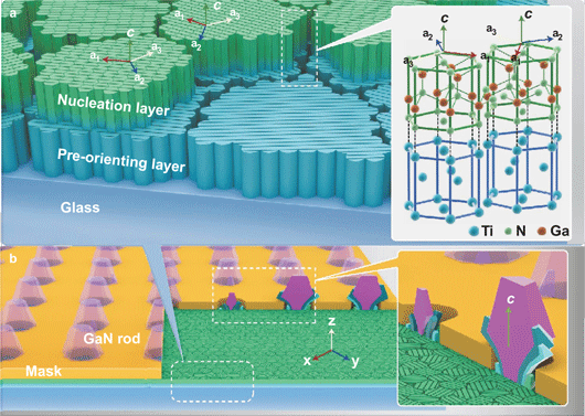
Figure 1: Schematic for fabricating GaN pyramid arrays. (a) Preferential polycrystalline morphology of titanium pre-orienting layer and LT-GaN nucleation layer. Inset: corresponding atomic arrangement of layers at the grain boundary. (b) GaN pyramid arrays formed during HT-GaN growth on oriented LT-GaN/titanium through patterned holes in SiO2 mask. Inset: during HT-GaN growth, the GaN pyramid formed from a few crystal islands grown predominantly with preferred c-axes in the z-direction.
Titanium grows with a hexagonal wurzite structure, like GaN, but with a lattice parameter mismatch of 7%. This mismatch is about half that of standard GaN on sapphire growth (~14%). The titanium grains tend to grow in columns, giving crystalline alignment in the vertical, but not lateral directions. Another potential advantage of using titanium in this way is its use as one of the electrodes in electronic devices. Titanium is also stable in ammonia/hydrogen at high temperature, unlike alternatives such as zinc oxide (lattice mismatch 1.9%) or aluminum nitride (-2.4%).
A silicon dioxide (SiO2) mask is used to allow local heteroepitaxy where the transfer of crystal orientation from the nucleation layer is constrained to a few orientations, creating near-single-crystal truncated pyramids (Figure 1b). The GaN in this stage is grown at a high temperature of 1040°C to ensure high crystallinity.
The diameters of the holes in the mask were varied between 0.2μm and 2.4μm. At larger sizes, the GaN grew with a central pyramid along with a few small fragments resulting from growth on nucleation sites of differing orientation. At 0.7μm diameter, almost all the smaller fragments disappeared, giving nearly-single-crystal GaN pyramids. One disadvantage of the smaller mask hole is reduced symmetry and order of the pyramid shape; the researchers say that they are still optimizing the process to improve this aspect.
The researchers formed five-period InGaN/GaN quantum wells on the pyramid arrays with ultraviolet photoluminescence (PL) peaks at 364nm with 16nm full-width at half maximum (FWHM). This FWHM performance is similar to that of GaN pyramids on sapphire, but single-crystal GaN films give a typically narrower 10nm. The internal quantum efficiency, estimated from PL measurements in the 10–300K range, is given as 52%.
The team comments: “This value of IQE (a typical measure of recombination defect centers) clearly demonstrates the excellent crystalline property of the arrays. The high IQE may be attributed to the reduced quantum-confined Stark effect (QCSE) of the (10-11) semi-polar facets as well as the high crystallinity in this region, where the MQWs were formed.”
The decay time in time-resolved measurements was 2.61ns. The researchers thus attribute 5.02ns (2.61ns/0.52) to radiative decay, and 5.44ns to non-radiative (2.61ns/0.48).
Indium tin oxide (ITO) was used as a transparent conductive layer on top of p-GaN deposited on the multi-quantum well (MQW) pyramids for electroluminescence (EL) measurements, creating LEDs (Figure 2a). The region between the pyramids was filled with 3μm spin-coated insulating AZ1512 polymer (a photo-resist) before ITO deposition. The n-electrode consisted of the bottom titanium pre-orienting layer, which also served as a reflector. Although the researchers describe the structure as being efficient in light extraction, “transmittances of other layers need to be further improved”.
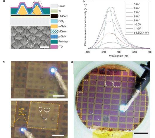
Figure 2: Crystal quality of GaN pyramid arrays and electroluminescence devices fabricated on top of GaN pyramid arrays. (a) Electroluminescence device structure (upper panel) and its corresponding SEM image (bottom panel). (b) Electroluminescence spectra at different voltages and of the s-LED at 3.1V. The peak intensity of the s-LED spectrum was normalized to that of the electroluminescence device spectrum. (c, d) Photographs of electroluminescence at different locations, showing bright, surface-type emission. Scale bars, 5mm (a, bottom panel), 0.5cm and 1cm (c and d, respectively).
The EL spectra were much broader than for single-crystal devices (Figure 2b). Also, the peak wavelength varied across the facets of the pyramids. The peak wavelength was 478nm at the rod apex, decreasing to 448nm towards the pyramid base. These wavelengths are in the ‘blue’ region (440–490nm) of the visible spectrum. The wavelength decrease is attributed to indium composition and MQW thickness variations.
The researchers add: “On a macroscopic scale, we observed quite uniform and surface-type electroluminescence emission at different locations [Figures 2c, 2d]. To the best of our knowledge, this is the first demonstration of such electroluminescence emission from GaN grown on glass.”
With the vertical current injection allowed by use of the titanium electrode, the current crowding of the usual lateral injection on insulating substrates like sapphire (and glass) is avoided. Such current crowding tends to degrade LED performance/efficiency.
The maximum luminance was 600cd/m2, which is almost half the value for the same MQW structure deposited on a single-crystal substrate. “This suggests the possibility of achieving brighter and efficient electroluminescence devices by adopting a standard LED layer structure with an electron-blocking layer,” the researchers comment.
Since the research is only at the proof-of-concept stage, there are many possible improvements such as reducing leakage currents through further optimization.
Pyramid LEDs Amorphous glass GaN InGaN MOCVD
The author Mike Cooke is a freelance technology journalist who has worked in the semiconductor and advanced technology sectors since 1997.