- News
7 September 2011
Tegal sets bid deadline for Nanolayer Deposition patent portfolio
Tegal Corp of Petaluma, CA, USA says that bids for its intellectual property portfolio for nanolayer deposition (NLD) technology will be accepted until 5pm PDT (pacific daylight time) on 30 September. The firm established the bid deadline after several major IC and semiconductor equipment manufacturers expressed interest in the IP portfolio. The deadline is subject to being extended or withdrawn.
In March 2010, Tegal sold its legacy thin-film etch and physical vapor deposition (PVD) product lines to OEM Group Inc of Gilbert, AZ, USA for up to $3m. This February, it sold its deep reactive ion etch (DRIE) assets to plasma etch, deposition and thermal processing equipment maker SPP Process Technology Systems Ltd (SPTS) of Newport, Wales, UK. Now, through its investment in sequel Power, Tegal is engaged in the promotion of solar power plant development projects worldwide and other renewable energy projects.
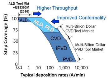 Graphic: Tegal’s NLD bridges performance gap in deposition technologies for semiconductor production.
Tegal says that NLD process technology bridges the gap between high-throughput, non-conformal chemical vapor deposition (CVD) and highly conformal, low-throughput atomic layer deposition (ALD). The portfolio includes more than 35 US and international patents in the areas of pulsed-CVD, plasma-enhanced ALD, and NLD.
“Advanced chip designs often require increased process flexibility over the current deposition technologies to achieve performance goals and to maintain broad process windows,” says chief technologist Robert Ditizio. “Tegal’s NLD portfolio provides a number of options for extending the life of conventional CVD process hardware without the need to move completely to lower-throughput ALD processes,” he adds.
NLD and pulsed-CVD processes have been developed to fill the gap that was created as IC manufacturers moved from conventional CVD to ALD. Although ALD has proven an effective process technology for applications requiring highly conformal film deposition, the conformality has come at the expense of throughput, says Tegal.
Conformal film deposition technology is a key component of advanced metallization schemes, through silicon vias (TSVs) and LED manufacturing, among other applications, but NLD technology also provides unique process capabilities for depositing nanolaminate and composite films without the precursor supply limitations imposed with ALD, claims Tegal. The deposition of high-k dielectrics and other complex oxides, and of films of tertiary alloys such as GeSbTe used in phase-change memories for example, can benefit from the process latitude available with NLD, the firm adds. While ALD process developers are sometimes hampered by the need to find reactive saturating precursor combinations for ALD process windows that are closely matched in temperature for each element in a film stack, NLD technology uses plasma treatment steps (in place of paired chemical reactants) to overcome this limitation, allowing for increased process latitude in the fabrication of complex dielectric films and metal alloys, concludes Tegal.
Tegal sells thin-film etch and PVD assets to OEM Group