- News
23 April 2012
More polarization engineering enhancement in nitride semi HFETs
German researchers have reported further results of their polarization engineering for nitride semiconductor heterostructure field-effect transistors (HFETs) [N Ketteniss et al, Semicond. Sci. Technol., vol27, p055012, 2012]. The aim of the work is to create HFETs with positive threshold voltages, therefore allowing normally-off (enhancement-mode) operation.
Normally-off devices are especially desired in power applications for fail-safety and for lower power consumption. Without special processing, such as gate recessing or fluorine plasma treatment, nitride semiconductor HFETs usually operate in ‘depletion-mode’ with normally-on behavior, where a current flows at zero gate potential.
A few weeks ago, RWTH Aachen University and Fraunhofer IAF (Institute for Applied Solid State Physics) reported on the use of quaternary indium aluminum gallium nitride (InAlGaN) as the barrier material for HFETs that allows lower interface polarization charge to be achieved with an underlying GaN channel/buffer layer (Polarization matching as a route to nitride semiconductor transistor enhancement ). The lower charge shifted the threshold to the enhancement region.
There is also a further advantage in having reduced interface charge when producing metal-insulator-semiconductor HFETs (MISHFETs) to reduce gate leakage currents. When insulator is applied to the HFET structure, it tends to shift the threshold in a negative direction. The effect is proportional to the interface polarization charge.
The new report also involved RWTH Aachen University, along with Forschungszentrum Jülich GmbH and Jülich Aachen Research Alliance (JARA-FIT).
The epitaxial material was produced on sapphire in an Aixtron AIX 200/4 RF-S metal-organic chemical vapor deposition (MOCVD) system. An AlN nucleation layer was deposited at 780°C. The buffer consisted of 300nm AlN and 2.5μm GaN, grown at 1250°C and 1070°C, respectively. The further barrier layers (Figure 1) of AlN and InAlGaN were grown at 805°C.
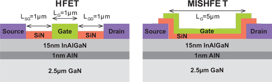
Figure 1: Schematic cross section of the investigated devices. Left: SiN passivation layer has a thickness of 120nm. Right: SiN gate insulator is 20nm thick.
Rutherford backscattering spectroscopy study of a thicker barrier than used for the transistors gave the composition of the quaternary InAlGaN barrier as 2% In, 16% Al, and 82% Ga. The researchers estimate that the residual interface charge density was 0.0075C/m2, the bandgap of the barrier was 3.66eV, and that the conduction band offset was 0.24eV from that of the GaN buffer layer.
This compares with a ternary AlGaN barrier with 10% Al that gives a structure with a residual interface charge density of 0.0063C/m2 but a lower conduction band offset of 0.19eV. The researchers comment: “Keeping the conduction band offset reasonably high while reducing the interface charge σpol can only be realized in the quaternary material system. Hence, the In content in our devices helps us to reduce σpol while maintaining a specific bandgap.”
The epitaxial material was processed into both HFETs and MISHFETs. Mesa isolation was realized using chlorine-based plasma etch. Ohmic source-drain contacts consisted of 825°C-annealed titanium/aluminum/nickel/gold. Silicon nitride (SiN) was used as 120nm passivation for the HFET and 20nm gate insulation for the MISHFET. The gate metals were nickel/gold.
The HFET had a gate length of 1μm with 3μm source-drain separation. The MISHFET gate overlapped the source-drain contacts that were separated by 5μm. The MISHFET gate overlap was designed to ensure carrier accumulation over the whole channel length and thus to reduce the on-resistance
The transistors were tested at 4V drain bias (Figure 2). For the HFET, the drain current was 205mA/mm at 2V gate potential. The gate current was as low as 0.15mA/mm. The threshold voltage of the device was 0.05V, giving normally-off behavior. The peak transconductance was 130mS/mm.
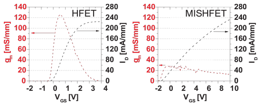
Figure 2: Typical transfer characteristics measured at 4V drain bias: left, for the HFET device; right, for the MISHFET device.
The researchers see these as impressive results ‘out of the box’, commenting in addition that “A more sophisticated device structure and optimized barrier design will easily improve the device characteristics further and also provide a more positive threshold voltage.”
The MISHFET had a negative threshold voltage shift of -1.3V, compared with the HFET. This is attributed to the heterostructure still having some interface charge. However, this shift is small compared with AlGaN/GaN MISHFETs with 8nm of SiN insulator that have shifts of more than -3V.
The researchers comment: “Choosing a barrier layer composition which is even closer to the polarization-matched case would prevent such a shift and enable even higher threshold voltages for both the HFET and the MISHFET concept.”
Since the MISHFET has a longer gate of 5μm, the transconductance is lower. Despite this, the device does achieve drain currents beyond 200mA/mm with less than 0.5mA/mm gate leakage at 7.6V gate potential.
The researchers expect improvements from using atomic layer deposited (ALD) aluminum oxide in place of the SiN gate insulation. They also believe that optimization of the MISHFET design is needed, since the metal-insulator-metal structure over the ohmic source-drain contacts is not ideal. Possibly, the polarization engineering technology with insulated gate could benefit from being implemented in a vertical device such as the current-aperture vertical electron transistor (CAVET) structure.
Polarization matching as a route to nitride semiconductor transistor enhancement
HFETs MISHFETs InAlGaN barrier MOCVD GaN AlN Aixtron
http://iopscience.iop.org/0268-1242/27/5/055012/
The author Mike Cooke is a freelance technology journalist who has worked in the semiconductor and advanced technology sectors since 1997.