- News
30 April 2012
AlGaN buffers on semipolar GaN offer new route to UV LDs
University of California Santa Barbara (UCSB) has developed ultraviolet (UV) laser diodes (LDs) based on semipolar aluminum gallium nitride (AlGaN) buffer layers [Daniel A. Haeger et al, Appl. Phys. Lett., vol100, p161107, 2012]. The aim was to provide an alternative route to UV LDs compared with those grown on AlN or sapphire substrates.
Potential commercial and industrial applications include bio-agent detection, chemical processing, photo-lithography, and sterilization/purification. Using LDs in these applications should increase power efficiency, make for more compact equipment, increase reliability, and significantly reduce capital and operating costs compared with traditional UV lasers.
With nitride semiconductor light-emitting devices, the reduction of defect densities is usually one of the key steps to high performance. Since the materials are often grown on substrates with different lattice parameters from that of the light-emitting region, they are prone to contain threading dislocations.
UCSB has been developing AlGaN buffer layers on semipolar GaN as a means to transition between the substrate lattice constant and that of the active region. The researchers have found that such buffer layers relax plastically through misfit dislocations near the heterointerface, offering “the potential for significantly higher-quality AlGaN pseudo-substrates at any Al-mole fraction”.
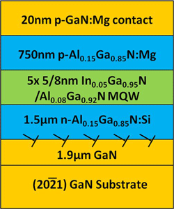 The new UV LD structures were grown on free-standing (20-21) GaN substrates supplied by Mitsubishi. (Kenji Fujito of Mitsubishi Chemical Corp is the only non-UCSB representative on the paper’s 11-author list.) Metal-organic chemical vapor deposition (MOCVD) was used to grow the nitride layers of the laser (Figure 1). The growth conditions and doping were not optimized.
Figure 1: Schematic cross section of the laser diode epitaxial structure. Stress relaxation occurs only at the GaN/n-AlGaN interface by the formation of misfit dislocations. There is no electron-blocking layer.
The epitaxial material was processed into various ridge-waveguide LDs. The ridge direction was [10-14]. The facets were not coated.
X-ray analysis of the epitaxial material suggests that the strain between the substrate and AlGaN buffer is indeed relaxed through misfit dislocations. The researchers found that the only relaxation was at the GaN/n-AlGaN interface, with no measureable secondary relaxation at the p-cladding or active region interfaces.
Transmission electron micrographic (TEM) studies give an upward limit for threading dislocation density in the laser structure of mid 107/cm2, comparable to the density value for the GaN substrate and one magnitude lower than that for AlGaN films grown previously.
The resulting devices had UV lasing frequencies of 384nm. A 5μm x 1500μm device had a threshold current of 1.17A (15.7kA/cm2 density), threshold voltage of 13.7V, and slope efficiency of 0.061W/A (Figure 2).
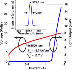 Figure 2: Dependence of output power and voltage on current under pulsed operation. Inset: output spectra at lasing threshold.
Temperature-dependent measurements gave a characteristic temperature of 91K for 2.5μm x 1200μm devices, lower than for visible nitride LDs but comparable to the values for previously reported UV LDs.
Cavity-length-dependent measurements suggest a low carrier injection efficiency of less than 3%. The researchers comment: “We speculate that this low injection current is due to defects near the active region/p-cladding interface as well as low electron barrier heights. We believe this can be mitigated with growth condition optimization and improved carrier confinement structures.”
Internal modal losses were also high, at more than 60/cm. “It is clear that extensive optimization of the waveguide structure to reduce the optical mode width and thus the internal losses will be critical for the reduction of threshold current densities and for the realization of deeper UV LDs,” the researchers write.
The team hopes to “significantly improve the optical confinement” by reducing the stress relaxation of the cladding/waveguide layers at given alloy composition and increasing the lattice constant of the epilayers. This will allow the maximum thickness of layers to be increased and alloy composition contrast to be enhanced in the active light-emitting region.
The work received funding from US Defense Advanced Research Projects Agency (DARPA) Compact Mid-Ultraviolet Technology (CMUVT) program and the Solid State Lighting and Energy Center (SSLEC) based at UCSB.
The author Mike Cooke is a freelance technology journalist who has worked in the semiconductor and advanced technology sectors since 1997.