- News
11 April 2012
First strained GaN quantum well transistor with AlN barriers
University of Notre Dame has realized the first strained gallium nitride (GaN) quantum well (QW) transistors with unstrained aluminium nitride (AlN) barriers [Guowang Li et al, IEEE Electron Device Letters, published online 12 March 2012].
One hope of using ultra-thin-body (UTB) structures such as QWs is to avoid the many short-channel effects that degrade transistor performance when scaled to smaller dimensions. Silicon devices have used amorphous dielectrics such as silicon dioxide to create UTB layers of silicon on insulator. However, these materials are thermally insulating. Using epitaxial AlN as electrical insulator for GaN channels does not have this drawback since its thermal conductivity is high at 3.4W/cm-K. By contrast, the thermal conductivity of silicon dioxide is reduced from this by two orders of magnitude, at around 1.4W/m-K (0.014W/cm-K).
The nitride heterostructures (Figure 1) were produced using molecular beam epitaxy (MBE) on 1μm-thick semi-insulating metal-polar AlN templates on sapphire substrates. A further 210nm of AlN was grown as a buffer before the 23nm GaN quantum well layer. The final AlN barrier and GaN cap were 4.5nm and 2.5nm, respectively. The cap layer was designed in to protect the AlN surface from oxidation.
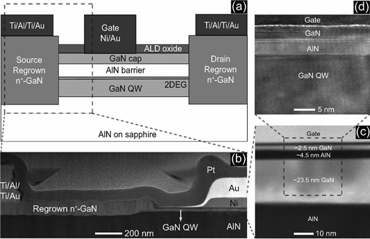
Figure 1: (a) Schematic of device structures (not to scale). (b) Z-contrast STEM image of gate-to-source regions, showing re-grown GaN connected to the GaN QW channel. (c) Z-contrast STEM image of active layers under the gate, resolving the sharp interfaces between binary III nitrides. (d) HRTEM image of top AlN/GaN QW interface at the 2DEG channel region.
Hall mobility measurements on the structure give a rather low figure of 280cm2/V-s. However, the researchers expect to be able to improve this by increasing the growth temperature and/or changing the growth rate.
The two-dimensional electron gas (2DEG) density of 1.77x10¹³/cm2 is lower than that usually achieved with 4.5nm/2.5nm AlN/GaN top barriers. The researchers say that this is due to the GaN layer on AlN being under compressive strain, which results in a piezoelectric polarization that opposes the spontaneous polarization. The negative polarization charge at the bottom GaN/AlN interface may also deplete the 2DEG.
The AlN back-barrier also has enhanced thermal dissipation compared with InGaN or AlGaN, which are more often used in the nitride semiconductor heterostructures.
The source and drain regions of the transistor were formed by etching and re-growing 120nm GaN regions with heavy silicon doping to give high n-type conduction. Silicon dioxide was used as an etch mask. The re-growth was performed using MBE. Surface passivation was achieved with atomic layer deposition (ALD) of 1nm of aluminium oxide and 6nm of hafnium dioxide.
The gate was 2.1μm in length and 49.5μm wide. The gate-source and gate-drain separations were 0.4μm and 6.9μm, respectively.
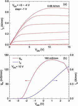 At 10V drain bias, the device pinched off at -2.4V with a drain current density of less than 1mA/mm (Figure 2). The saturated drain current at +3V was 0.68A/mm. The peak transconductance was 160mS/mm. The drain-induced barrier lowering (DIBL) of 40mV/V (exhibiting a ‘long-channel’ behavior) was extracted from drain biases of 0.5V and 10V.
Figure 2: (a) Output characteristics of GaN QW device with gate length of 2.1μm. (b) Transfer characteristics at 10V drain bias.
At a forward gate potential of 15V and a drain bias of 10V, the buffer leakage was 0.5mA/mm and the subthreshold slope was 400mV/dec. The poor subtheshold behavior was possibly due to unintended dopants and traps in non-optimal buffer layers.
The researchers comment: “Although the device performance lags current state-of-the-art GaN HEMTs, it is important to note that this is the first realization of a novel device structure that offers substantial opportunities for scaling. By scaling down the thicknesses of the GaN QW and/or top AlN barrier, an enhancement-mode operation can be a natural outcome in a self-aligned device.”
The researchers also believe that different QW channels with lower (InGaN) or higher (AlGaN) bandgaps would allow scaling to high speed or high breakdown voltage, respectively. They also see the full benefit of the structure being achieved with the use of bulk AlN substrates rather than the demonstrated AlN template layers on sapphire.
The research was supported by the US Defense Advanced Research Projects Agency (DARPA) NEXT program (www.darpa.mil) the US Air Force Office of Scientific Research (AFOSR) and the US Office of Naval Research (ONR) DATE program.
GaN Quantum well transistor AlN barriers ALD MBE
The author Mike Cooke is a freelance technology journalist who has worked in the semiconductor and advanced technology sectors since 1997.