

- News
22 August 2012
GaN-on-Si large-signal performance beyond 40GHz
Researchers in Switzerland and the USA have reported the first large-signal performance for a gallium nitride on silicon (GaN-on-Si) high-electron-mobility transistors with output power density of 2W/mm and associated peak power-added efficiency (PAE) of 13.8% (peak 18.5%) at 40GHz without field plates [Diego Marti et al, IEEE Electron Device Letters, published online 9 August 2012]. The researchers also claim the highest cut-off frequencies to date for fully passivated AlGaN/GaN HEMTs on silicon substrates.
Four of the researchers are with the Millimeter-Wave Electronics Group, ETH Zürich, and one other is with Nitronex Corp, the supplier of the nitride semiconductor on silicon layers. The substrate was 100mm float-zone refined Si (111) that had a high resistivity (10kΩ-cm). The layers consisted of: a nucleation/transition layer, a 1.7μm GaN buffer, a 1nm aluminium nitride (AlN) spacer, a 17.5nm AlGaN barrier, and a 2nm GaN cap. This resulted in a material with improved mobility of 1500cm2/V-s and a crack-free surface.
The transistors were formed with 850°C annealed titanium/aluminum/molybdenum/gold ohmic source-drain contacts, mesa isolation, a recessed nickel/platinum/gold T-gate (200nm high, 500nm wide) in the center of the source-drain gap, 75nm silicon nitride passivation, and titanium/gold contact pads.
A range of HEMTs were produced (Table 1). For example, a HEMT with a 100nm gate length in a 1μm source-drain gap had a maximum drain current of 1.05A/mm at 2V gate potential and a maximum transconductance of 540mS/mm (for drain bias of 5V and gate potential of -0.5V). The Schottky gate diode leakage was 300μA/mm at -5V gate voltage. The gate-drain breakdown (1mA/mm) occurred at 29V.
Pulsed measurement to assess current-collapse/gate-lag effects showed little dispersion, indicating low-damage impact from the processing despite the deep recessing used. The researchers comment: “The drain lag is moderate and can be attributed to the surface SiN passivation as well as the improved channel confinement associated with the AlN spacer.”
Small- and large-signal radio frequency measurements (0.2-40.2GHz) were carried out. The small-signal investigations of a 75nm gate-length device resulted in cut-off frequencies (fT) of 125GHz and maximum oscillation (fmax) of 145GHz before de-embedding.
Making de-embedding corrections at a drain bias of 2.6V and gate bias of -0.5V, using extrapolations of Mason’s unilateral gain parameter, gave fT of 152GHz and fmax(U) of 149GHz. The researchers comment: “This fT is the highest value ever reported for any GaN HEMT on silicon, exceeding the previous record established using AlInN/GaN HEMTs, providing a 42% improvement with respect to our previous 75nm AlGaN/GaN-on-Si devices.”
The corresponding results for a gate length of 100nm were an fT of 120GHz and fmax(U) of 140GHz (3V drain, -0.4V gate).
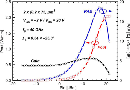
Figure 1. Power sweep of 200nm-gate HEMT at 40GHz at bias conditions of −2V gate and 20V drain. The device showed a maximum output power of 2.05 W/mm and a peak PAE of 18.5%.
The frequency performance is also maintained at the drain biases needed for large-signal operation. The devices were tested at 40GHz in a set-up with a nonlinear vector network analyzer (Agilent PNA-X NVNA) source and load-pull. A 200nm gate-length device with 2μm source-drain gap had maximum power output density of 2.05W/mm and corresponding power-added efficiency (PAE) of 13.8%. At a lower power output density of 1.8W/mm the PAE peaked at 18.5% (Figure 1). The gate leakage was 0.3mA/mm during operation.
In general, the longer gates give better large-signal performance (Table 1). “The results confirm GaN-on-Si technology as a promising contender for low-cost millimeter-wave power electronic applications,” the researchers write.
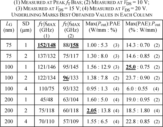
Table 1. Large- and small-signal parameters.
Although better performance can be obtained on much more expensive silicon carbide substrates, there is much interest in GaN-on-Si for wider application in high-frequency high-power electronics. According to the researchers, there have been no reports of large signal for GaN-on-Si beyond 20GHz until now. However, low-noise performance has been reported in recent weeks.
Reducing noise at high frequency in nitride-on-silicon transistors
Tags: GaN/Si HEMTs
The author Mike Cooke is a freelance technology journalist who has worked in the semiconductor and advanced technology sectors since 1997.