

- News
26 December 2012
Reducing gallium nitride growth temperature to 500°C
Seoul National University and Ritsumeikan University in Korea have developed a new technique for growing higher-quality gallium nitride (GaN) layers at temperatures as low as 500°C [In-Su Shin et al, Appl. Phys. Express, vol5, p125503, 2012]. The work developed from the group’s previous observations in research directed towards higher-quality indium nitride (InN) and indium gallium nitride (InGaN) growth.
The new growth technique uses a pre-deposition of a thin layer of indium that improves the quality of the subsequent GaN. The indium apparently allows the Ga atoms to migrate more easily on the growth front and to become incorporated into the crystal structure. The indium is not incorporated, but rather is swept upward as the GaN layer develops.
The researchers see their technique as having potential application for growing large-bandgap GaN layers on narrower-bandgap InGaN. Such structures would be useful in multi-junction solar cells, for example. High-temperature growth on InGaN surfaces is difficult because the indium content then tends to evaporate due to its lower binding energy with nitrogen compared with gallium.
The growth temperatures for InN and GaN reflect this: for GaN molecular beam epitaxy (MBE) the normal growth temperature is around 750°C, while the maximum values for InN are 570°C (N-polar) and 470°C (In-polar). Growth of GaN at temperatures consistent with InN tends to result in low-quality polycrystalline layers with large numbers of misfit defects.
The researchers used MBE rather than metal-organic chemical vapor deposition (MOCVD), since MBE allows lower-temperature growth in general. Radio-frequency MBE was performed on 3μm semi-insulating GaN templates previously grown on sapphire substrates using MOCVD.
The researchers began RF-MBE with a thin layer of 700°C GaN to suppress surface oxidation effects. The temperature of the system was then lowered to 500°C or 550°C. The low-temperature (LT) 300nm GaN growth was preceded by a thin layer of metallic indium (In). After the LT GaN growth, the surface of the sample was cleaned of In residue with a hydrochloric acid treatment. Comparison samples without In pre-deposition were also made.
The growth of GaN rather than InGaN is due to the preferential incorporation of gallium rather than indium in the GaN crystal when a Ga-rich growth condition is used (N/Ga < 1). By contrast, in nitrogen-rich conditions (N/Ga >1), x-ray diffraction scans reveal peaks for both GaN and InGaN crystal regions. Scanning electron micrographs taken after the growth showed the presence of In droplets on the surface of the samples, indicating that the In-layer is swept out to the surface throughout the growth so long as Ga-rich growth is maintained.
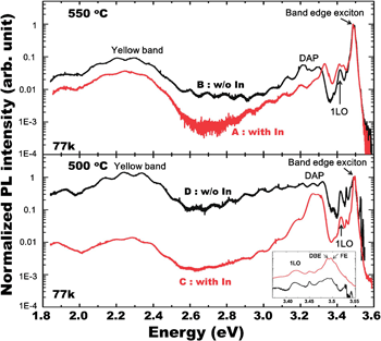 The samples were also subjected to photoluminescence (PL) excitation with a 325nm He-Cd laser at 77K (Figure 1). A strong band-edge signal at 3.48eV indicated again that the In was not incorporated into the crystal structure. Further, the samples with In pre-deposition show reduced ‘yellow band’ emission that has been associated with donor–acceptor transitions due to defects and impurities. By contrast, the yellow band for the lowest-growth-temperature GaN (500°C) without In pre-deposition (sample D) is higher intensity than the weak band-edge emission. The In pre-deposition (sample C) increases the band-edge by about 120 times, effectively suppressing the yellow band by about two orders of magnitude.
Figure 1: 77K PL spectra of LT GaN grown at (a) 550°C and (b) 500°C. (DAP: donor acceptor pair transition; LO: longitudinal optical phonon; DBE: donor bound exciton; FE: free exciton).
Another effect of In pre-deposition is to narrow the band-edge peak full-width at half maximum (FWHM) from 21meV to 14meV. On closer examination, the band-edge peak in sample C consists of two types of exciton – one is donor bound (DBE) and the other is free (FE). This structure of the band-edge is not clear in sample D.
The higher-growth-temperature GaN (550°C) also shows improvement in performance with In pre-deposition, although the yellow-band suppression is only a factor of 2.7 and the band-edge excitation is increased by 1.4x. The band-edge linewidth FWHM narrowing is also less impressive from 16meV to 14meV.
Hall measurements reveal almost an order of magnitude reduction in residual electron concentration and a modest increase in mobility with In treatment for the 550°C GaN (Table 1). The changes for the 500°C GaN are in the same direction, but not as dramatic.
| Sample | Growth temperature (°C) | In coverage | Hall mobility (cm2/V-s) | Hall electron concentration (/cm3) | Intensity ratio of yellow emission to band-edge 77K PL | FWHM of band-edge 77K PL (meV) | Root-mean-square AFM surface roughness (nm) |
| A | 550 | Yes | 200 | 2:2x10¹⁷ | 0.011 | 14 | 1.2 |
| B | 550 | No | 160 | 1:2x10¹⁸ | 0.030 | 16 | 1.4 |
| C | 500 | Yes | 152 | 9:8x10¹⁷ | 0.0044 | 14 | 1.3 |
| D | 500 | No | 149 | 1:1x10¹⁸ | 0.427 | 21 | 2.2 |
Table 1: Summary of experimental samples and results.
The surface texture of the samples was studied with atomic force microscopy (AFM). All the samples indicated that most of the growth proceeded in the ‘3D island mode’. However, with In treatment the samples were smoother and some regions showed evidence of 2D growth sporadically between the 3D islands. “These results demonstrate that the reduced surface migration at low temperatures was compensated by using the pre-deposited In,” the researchers comment.
Increased surface migration in GaN grown at higher temperatures leads to better crystal quality. The researchers point out that their material was not expected to have the performance of high-temperature GaN. They add: “However, our results, namely the improved structural, electrical, optical and surface properties of LT GaN epilayers with pre-deposited In, thoroughly indicate that this growth method can be employed to overcome the difficulties in obtaining good-quality LT GaN by the conventional growth methods.”
The author Mike Cooke is a freelance technology journalist who has worked in the semiconductor and advanced technology sectors since 1997.