

- News
18 December 2012
Distributed Bragg reflection in epitaxial nitride layers
Two Yale University researchers have developed epitaxial distributed Bragg reflectors (DBRs) in nitride semiconductors with reflectivities of more than 98% [Danti Chen and Jung Han, Appl. Phys. Lett., vol101, p221104, 2012]. Further, the structure used consisted of just four periods of gallium nitride (GaN) and air gaps produced using electrochemical (EC) etching.
Epitaxial DBRs consist of layers of semiconductor with different refractive indices that create interference effects that reflect light back from the structure. With arsenide-based semiconductors, these structures can be used to confine light in vertical-cavity surface emitting lasers (VCSELs), due to the large variation in the refractive index of aluminium gallium arsenide (AlGaAs) with aluminium fraction. DBRs are also used in spontaneous emission devices (resonant-cavity light-emitting diodes, or RCLEDs).
For nitride-based VCSELs, the refractive index variation in AlGaN is much smaller, meaning that, for high reflectivity, one needs 20‑40 different layers of semiconductor. Because of the difficulty in producing such structures with the required quality, recent developments of nitride-based VCSEL have used separately grown dielectric stacks for the DBR sections of these devices. Separate processing adds to manufacturing complexity, increasing production costs.
The Yale DBR is based on the large difference in refractive index between GaN (~2.5) and air (1). The structures for the DBR were grown using a standard two-step metal-organic chemical vapor deposition (MOCVD). The epitaxial material consisted of four pairs of undoped and n-type silicon-doped GaN layers. These were grown on a 500nm u-GaN spacer/etch-stop layer. The ground-plane underneath the structure consisted of 500nm n-GaN that was designed to ensure uniform distribution of the anode bias across the sample.
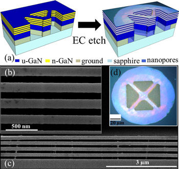 Figure 1: (a) Schematic of DBR fabrication process; (b) and (c) cross-sectional SEM images of GaN membrane DBRs confirming clear air gaps are formed; (d) differential interference contrast microscopy (DIC) image of DBRs after electrochemical etching. The formation of air gaps results in a circular pattern. The outer circle is the air gap of the DBR, while the inner circle is the unintentional porosification of the ground-plane layer.
Due to the higher conductivity of the n-GaN, the electrochemical etch proceeds selectively into these layers, giving air gaps between the unetched u-GaN layers. The thicknesses of the u-GaN were quarter or three-quarter wavelengths, where the target wavelength was ~500nm. The thickness of the n-GaN layer was quarter-wavelength with a view to mechanical stability of the eventual air gap.
The etching was carried out by first applying a vertical inductively coupled plasma reactive-ion etch (ICP-RIE) to expose the side walls of the structure for the subsequent lateral wet EC under-etch. The plasma etch was performed with a nickel mask. The electrolyte for the electrochemical etch consisted of ethanol/glycerol in hydrofluoric acid.
The quality of the structures was affected by both ICP-RIE and EC processes. In particular, the ICP-RIE needed to result in side-walls with minimal corrugation. For the EC etch, anode potentials below 15V result in smoother surfaces at the cost of a lower etch rate. At 12V, the surface roughness was less than 5nm root mean square over a 5μm x 5μm area.
The four-pair quarter-wavelength membrane structure achieved a peak reflectance of 98% at 503nm wavelength. The stop-band width was around 150nm. The researchers point out that the width of the stop-band was three to five times that of other reported epitaxy-based DBR mirrors. A simulation of the system suggests that fluctuation of the air-gap thickness degrades the performance somewhat.
The researchers also grew multi-quantum-well (MQW) superlattice structures on the DBRs and made photoluminescence measurements. The aim was to create a microcavity, as used in RCLEDs and VCSELs. The superlattice consisted of 30 pairs of In0.06Ga0.94N/GaN (2nm/2nm) and 10 periods of In0.17Ga0.83N/GaN (3nm/8nm) grown on a three-quarter-wavelength DBR designed for 460nm emission.
Photoluminescence on an excitation spot of diameter about 2μm showed significant line-width narrowing with a DBR, compared with the superlattice before EC etch (Figure 2). The full-width at half-maximum (FWHM) for the superlattice was 20nm without DBR and 17nm with DBR. Further, the emission intensity increased five to ten times with the DBR. The interference fringes also disappeared with the reduction in estimated cavity length to around 0.38μm.
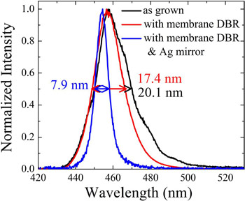 Figure 2: Emission spectra of MQW samples (1) without DBRs, (2) with bottom DBRs, and (3) with bottom DBRs and silver capping layer.
Although the reduction in FWHM is rather small, the researchers point out that this is due to the low reflectivity of the upper ‘mirror’ of the cavity (i.e. the top surface) of around 18%. By applying 50nm of silver to the top surface with reflectance of 70% at 460nm, the FWHM is reduced to less than 8nm.
The researchers carried out simulations with varying qualities of the bottom and top mirrors. Comparison of the results with the experimental FWHMs for 18% (bare top surface) and 70% (50nm silver) top mirror reflectivity suggests that the bottom mirror is highly reflective and compares favorably with the simulation involving a 95% reflective bottom mirror.
“The good agreement between the experimental and simulated FWHM with highly reflective bottom DBR indicates that the high-reflectance membrane DBR can be used to control the modes of spontaneous emission,” the researchers write.
By moving the position of the excitation spot from the unetched region of the structure across a strut to the central freely suspended region and out along an adjacent strut, the researchers were able to explore shifts in the peak frequency. The central, freely suspended region was blue-shifted some 35‑40meV relative to the response in the edge regions. The researchers believe the shift could be due to a reduction in strain leading to reduced piezoelectric fields in the MQW superlattice of the freely suspended region.
The strain relief was 0.104%, according to Raman shift measurements that are affected by differences in sound wave/phonon propagation with strain. The researchers used the change in strain/piezoelectricity to predict a peak wavelength shift of 34meV. “The good agreement between experimental and theoretical results suggests that the piezoelectric effect is the dominant factor responsible for the observed emission shift,” the researchers comment.
DBRs VCSELs AlGaAs RCLEDs GaN AlGaN MOCVD
http://link.aip.org/link/doi/10.1063/1.4768806
The author Mike Cooke is a freelance technology journalist who has worked in the semiconductor and advanced technology sectors since 1997.