- News
29 February 2012
Graphene-nanorod hybrid layer improves light emission and injection
Researchers in Korea have combined graphene (Gr) and zinc oxide nanorods (ZNRs) in a nitride semiconductor light-emitting diode (LED) transparent conducting layer (TCL) [Jung Min Lee et al, Appl. Phys. Lett., vol100, p061107, 2012]. The effect is to increase light emission, along with improving the electrical current injection performance of the device. The research was an academic-industrial collaboration between Hanyang University and LG Display Co Ltd.
At 2.8V forward bias, an LED with a Gr TCL demonstrated 4x the light intensity of a device without Gr, and 2x the injection current. Adding the ZNRs gave a further 66% light output.
The researchers believe that the TCL allows the current to spread over the full width of the device. Bare p-type gallium nitride (GaN) semiconductor has a lower conductivity, tending to restrict the current path to regions near the metal electrodes/pads. This creates a non-uniform current density across the device. High current densities tend to give less efficient light emission in nitride LEDs (efficiency droop).
The researchers comment: “Our hybrid approach, which combines the key advantages of both 1D nanostructures and 2D Gr, could open up advanced and new design opportunities in high-performance optoelectronic devices resulting in optimal performance and functionality.”
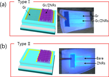 The base for the new device structure was a traditional InGaN LED with a trident-shaped p-electrode frame (Figure 1) to which a layer of graphene was applied. The graphene was produced by methane-based chemical vapor deposition (CVD) on copper and transferred to the LED surface. ZnO nanorods were then grown selectively on the graphene using a low-temperature hydrothermal process in aqueous solution.
Figure 1: Schematic diagrams and photographs of the type I and II LEDs. (a) Schematic of type I LED with Gr and Gr/ZNRs window electrodes, along with a photograph of the resulting device. (b) Schematic of type II LED with bare and ZNRs window electrodes, along with a photograph of the resulting device.
Optical experiments on the graphene and ZNR-graphene hybrid films suggested transmittances of 97% and 90% in the visible spectral range, respectively. The contact resistance was improved by including a very thin annealed layer of 1nm/1nm nickel/gold (Ni/Au) film before the ZNR-graphene hybrid film. The specific contact resistivity was reduced from 5Ω-cm2 to 0.5Ω-cm2 by the Ni/Au inclusion.
In all, four types of transparent conducting layers on the p-electrode were produced: a bare control, a ZNR-only film, a graphene film, and the ZNR-graphene hybrid. These were doubled up on two devices: ‘type I’ containing Gr-only and Gr-ZNR hybrid layers, and ‘type-II’ with bare and ZNR layers.
Scanning electron micrograph (SEM) inspection of the ZNR-graphene hybrid gave an average diameter for the near-vertical ZNRs of 50nm and an average height of 3μm. The hexagonal cross-section of the rods was taken as indicating high crystal quality. There was also observed a thin 50nm ZnO film immediately above the graphene and below the NRs. This thin layer is believed to act as a seed layer for the rods.
Further analysis with transmission electron micrography (TEM), energy-dispersive x-ray spectroscopy (EDS) and Raman spectroscopy confirmed that single-layer graphene remained stable at the metal/ZnO interface even after the hydrothermal process.
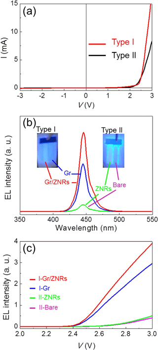 The turn-on voltages of the devices are around 2.5V (Figure 2a). At -3V reverse bias, the leakage current is 7x10⁻⁵A. Under higher forward bias, the grapheme-containing devices (‘type-I’) carry more current, due - it is thought - to more efficient current spreading by the graphene and thin metal layers.
Electroluminescence occurred around 446nm (Figure 2b). When driven at 2.8V, the current of the grapheme-containing devices was double that of the non-graphene devices (‘type-II’). In terms of light emission, the devices with graphene transparent contact exhibit up to 4x the amount of light intensity. Part of the improvement is attributed to reduced current crowding, giving more uniform illumination across the device. The improvement comes despite the estimated optical transmittance reduction of 20% due to the presence of the metal layers between the nitride contact and the graphene layers.
Adding the ZNRs increases the light intensity a further 66% over the graphene-only device. This improvement is attributed to multiple photon scattering and the more gradual change in refractive index between the GaN layer and air. ZNRs have also been used to improve light extraction with indium tin oxide (ITO) transparent conducting layers, giving a 57% boost with well-aligned rods and 34% for poorly aligned structures.
The better performance of ZNRs on graphene is attributed to the chemical stability of graphene. With ITO layers, the ZNR hydrothermal process attacks the transparent conducting layer, slightly degrading its electrical properties. ITO has further disadvantages such as limited indium supplies, and poor transparency at shorter blue and ultraviolet wavelengths.
Figure 2: (a) Current-voltage (I-V) curves of the type I and II LEDs. (b) EL spectra of the type I and II GaN LEDs with four different top window electrodes (I-Gr, I-Gr/ZNRs, II-bare, and II-ZNRs) recorded at an applied voltage of 2.8 V. (c) EL intensity vs voltage curves of GaN LEDs with different window electrodes.
The researchers also point to the better thermal properties of graphene for conducting heat away from the LED, improving performance.
Graphene nanorods Zinc oxide nanorods LEDs GaN
The author Mike Cooke is a freelance technology journalist who has worked in the semiconductor and advanced technology sectors since 1997.