- News
27 February 2012
Infrared nitride nanocolumn LEDs
Sophia University in Japan has produced 1.46μm infrared light-emitting diodes (LEDs) based on indium gallium nitride (InGaN) semiconductors [Katsumi Kishino et al, Appl. Phys. Express, vol5, p031001, 2012]. This was achieved by growing the nitride material in nanocolumns to allow the growth of a high-indium-concentration (~87%) active region and using a low indium concentration (~30%) for the hole-injection layer.
The new device approach not only brings optical communications within reach, it also raises the prospect of higher energy conversion efficiency nitride-based solar cells that can harvest a wider range of wavelengths.
Normally, InGaN LEDs are restricted to wavelengths shorter than green (570-520nm). This is because it is difficult to grow high-quality InGaN with the larger concentrations of indium needed to narrow the bandgap into the longer-wavelength ranges. In theory, the highest concentration (InN) should be able to emit at 1.95μm.
One reason for the difficulty in growing high-quality InGaN is that the InN and GaN materials do not mix well. Growing their alloy tends to result in clumping of high-concentration and low-concentration regions, somewhat like oil in water.
In addition to the difficulty in growing uniform-composition InGaN, a new factor appears at indium concentrations greater than 49%. In such material, a thin n-type ‘inversion layer’ appears at the surface, making it difficult to achieve p-type conductivity through the normal route of magnesium (Mg) doping.
The Sophia University researchers created a triangular array of n-GaN nanocolumns using selective-area growth (SAG) through a titanium mask in a radio-frequency molecular beam epitaxy (rf-MBE) process. The nanocolumn diameter was 325nm and the period of the triangular lattice was 350nm.
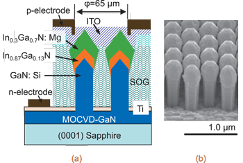 The nanocolumns were capped with 80nm InGaN active layers and 300nm p-InGaN cladding (Figure 1). The tops of the nanocolumns had a match-head appearance, with reduced spacing between the heads of less than 20nm.
Figure 1: (a) Cross-sectional schematic structure of near-infrared nanocolumn LED, and (b) scanning electron micrograph (SEM) bird’s-eye-view of LED crystal (sample B) taken at 55° angle from normal.
The p-InGaN layer had reduced indium content of 30% to avoid the problem of electron accumulation in an inversion layer at the surface that occurs in high-indium-content layers.
The full structure was about 1050nm high. The substrate/template consisted of GaN grown by metal-organic chemical vapor deposition (MOCVD) on sapphire.
Electrical contact was made with the tops of the nanocolumns with indium tin oxide (ITO) transparent conductor. The n-side contact was titanium/aluminum/titanium/gold.
The DC electrical performance varied with the magnesium (Mg) doping concentration of the p-InGaN layer, with only the highest-doped sample showing clear rectification behavior. Increasing the Mg beam pressure also resulted in rougher surface quality. The turn-on voltage for the highest-doped device was 1V. At 1mA (30A/cm2), the voltage was 3.5V.
Electroluminescence was measured using a filter to cut wavelengths shorter than 960nm. The peak emission of the device is in the near-infrared, at 1.46μm (Figure 2). The full-width at half-maximum (FWHM) was 157meV (~0.27micron). The emission intensity increased linearly with injection current between 1.46mA and 17.8mA.
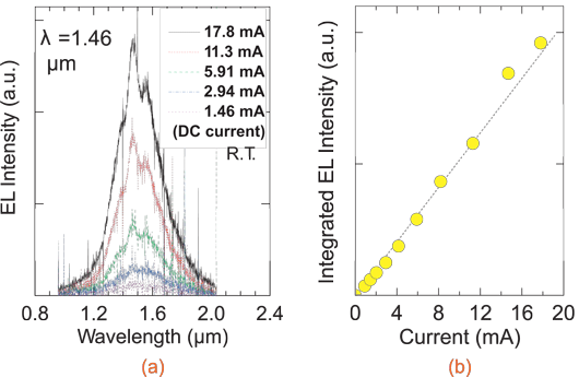
Figure 2: (a) Electroluminescence (EL) spectra of GaN-based nanocolumn LED with In-rich In0.86Ga0.14N active layer under DC current injection from 1.46mA to 17.8mA, and (b) integrated EL intensity vs current.
The emission wavelength leads the researchers to estimate the indium content of the active layer at 86%. The slight difference with the composition, as determined by transmission electron micrographic analysis, is attributed to compositional deviation between samples and/or ambiguity in the bowing parameter.
The researchers conclude: “We consider that this experimental finding is a step forward in the development of III–V-nitride-based infrared electrically driven emitters (e.g. LEDs and laser diodes) and photodetectors”.
Infrared LEDs InGaN LEDs MOCVD
http://apex.jsap.jp/link?APEX/5/031001/
The author Mike Cooke is a freelance technology journalist who has worked in the semiconductor and advanced technology sectors since 1997.