- News
10 February 2012
Longer-wavelength lasing in gallium antimonide heterostructure diodes
Researchers at Germany’s Technische Universität München have made room-temperature type-I quantum well (QW) gallium antimonide (GaSb) lasers with the longest emission wavelength yet reported [Kristijonas Vizbaras and Markus-Christian Amann, Semicond. Sci. Technol., vol27, p032001, 2012].
The wavelength of 3.7μm falls within the 2-4μm window that is of interest for the detection of methane, carbon dioxide, sulfur dioxide, ozone, etc. Detection of these gases is important for industrial and environmental monitoring. Tunable semiconductor lasers could result in compact low-cost systems.
Type-I QW structures are preferred where the wells confine both electrons and holes, since this increases overlap of the two types of carrier and hence radiative recombination. Conventional GaSb QWs tend to become type-II for energy bandgaps that would allow wavelengths longer than 3μm. Type-II means that the well for electrons is separated from the well for holes, reducing radiative recombination.
To overcome this problem, quintinary alloys of the five elements aluminum gallium indium arsenic antimony (AlGaInAsSb) have been developed to allow the extension of type-I wells to longer wavelength. TU München’s Markus-Christian Amann was involved in the first report in 2005 of such use of the AlGaInAsSb system for making room-temperature lasers with emission wavelengths of 3.26μm.
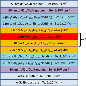 The laser material for the new 3.7μm device (Figure 1) with five type-I QWs was grown on gallium antimonide (GaSb) substrates in a Varian molecular beam epitaxy (MBE) reactor using solid sources for the group III (Al/Ga/In) metals and valved cracker cells for the arsenic (As) and antimony (Sb). The n- and p-type dopants were tellurium (Te) and beryllium (Be), respectively.
Figure 1: Schematic epitaxial layer structure of the investigated devices, emitting at 3.73μm.
The growth temperatures varied (according to layer) between 550°C for oxide removal, through 505°C for the lower and upper layers, and down to 450°C for the layers between and including the waveguides.
Material characterization indicated good material quality with no relaxation of strain. X-ray diffraction measurement indicated ~0.2% compressive strain in the waveguide layers. The strain is attributed to lack of control of As/Sb ratios during the growth steps involving both group-V materials.
The epitaxial material was processed into standard Fabry–Perot ridge-waveguide lasers with stripe widths in the range 22-30μm. The ridge was defined by wet etching down to the upper waveguide layer. The etched mesas were passivated with 240nm of sputtered silicon dioxide and contact windows were then opened in this layer using plasma etching.
The top metal contact consisted of titanium/platinum/gold. The backside of the wafer was thinned to 120μm using chemical mechanical polishing (CMP) and a back Ti/Pt/Au contact was applied.
The laser structures were cleaved into bars of different lengths (1-2.5mm). The mirror facets were ‘as-cleaved’, i.e. there was no further mirror processing such as the application of reflective coating. The bars were mounted epi-side up on copper heatsinks.
The devices were designed to emit at 3.73μm wavelength. The threshold current densities were in the range 1-3.5kA/cm2 at 20°C. The extrapolation to infinite cavity length was 676A/cm2, or 135A/cm2 per quantum well. Carrier broadening effects from diffusion outside the laser stripes were corrected for in these results. Without correcting for carrier broadening, the threshold current density for a device with a 2.4mm x 30μm ridge was 1.38kA/cm2 at a heatsink temperature of 20°C.
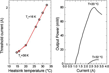 The thresholds were around 20% lower than the researchers’ previous results with 3.6μm laser diodes. The characteristic temperature of the threshold (Figure 2) was also higher than in the previous work, at 38K below 20°C and 16K above below 20°C. A higher characteristic temperature makes for more constant operation over a range of temperatures. The maximum operating temperature of 32°C was also higher than for the earlier device.
Figure 2: (a) Threshold current as function of heatsink temperature for 2.4mm-long devices with 30μm-wide ridges. Hollow circles are measurement points and red lines are exponential fits. (b) Pulsed power versus current (P–I) characteristics of the same laser at different temperatures.
The researchers attribute the improved performance to “considerably higher strain in the active region (1.46% compared to 1.05%), which leads to increased differential gain and lower transparency currents, thus counteracting the higher non-radiative losses”.
The change in characteristic temperature at 20°C is attributed to the onset of a non-radiative mechanism that is not yet completely understood. Two possibilities are hole leakage and Auger recombination.
A recent theory (http://link.aip.org/link/doi/10.1063/1.3646552) suggests that Auger electron‑hole recombination to an excited electron can be enhanced in systems with large conduction band offsets relative to the bandgap. The 3.7μm laser has an offset/bandgap ratio of 0.8, which is greater than the 0.5 needed for the suggested Auger enhancement, making it a candidate for such enhancement. Also, a further effect of higher temperatures is to shrink the bandgap, increasing the relevant ratio.
The two latest devices from Technische Universität München with wavelengths of 3.6μm and 3.7μm fall within the important water absorption-free window between 3.5μm and 4.5μm. This window could be important for the atmospheric detection of methane, ozone, and the silicon dioxide industrial pollutant.
The author Mike Cooke is a freelance technology journalist who has worked in the semiconductor and advanced technology sectors since 1997.