- News
9 January 2012
IMEC/AMAT produce first crack-free MOCVD nitride DH-structures on 200mm Si
IMEC and Applied Materials researchers say that they have shown for the first time that it is feasible to grow crack-free aluminum gallium nitride (AlGaN) double heterostructures (DH) with thick AlGaN buffer layers on 200mm silicon (Si) substrates using metal organic chemical vapor deposition (MOCVD) [Kai Cheng et al, Appl. Phys. Express, vol5, p011002, 2012]. Such DH structures are aimed at producing field-effect transistors (DHFET) with high breakdown voltage for next-generation power switching devices.
In creating DH wafers, the researchers were particularly keen to reduce wafer-bowing effects to less than 50μm, since that is the limit set by equipment designed for mainstream silicon complementary metal-oxide-semiconductor (CMOS) integrated circuit mass production.
Double heterostructures of Al0.35Ga0.65N/GaN/Al0.25Ga0.75N were grown on 200mm Si(111) wafers using an Applied Materials shower-head reactor. A 220nm AlN nucleation layer was grown first, followed by two intermediate layers of Al0.75Ga0.25N and Al0.5Ga0.5N, before the thick buffer of Al0.25Ga0.75N. The purpose of the intermediate layers was to counter-balance thermal tensile stress in the nitride layers imposed by the silicon substrates.
Previous work with only a single intermediate layer of Al0.45Ga0.55N had a radius of curvature of wafer bowing out to 40 meters, but this needed to be extended further to beyond 100 meters to meet the 50μm specification. With GaN buffer layers, it had been found that a single Al0.5Ga0.5N layer allowed 2.3μm-thick GaN wafers to be produced with less than 20μm wafer bowing.
Sample |
Al0.5Ga0.5N/Al0.75Ga0.25N thickness (nm) |
Al0.25Ga0.75N thickness (nm) |
Wafer bow (μm) |
Al0.25Ga0.75N (002) |
Al0.25Ga0.75N (102) |
A1 |
200/200 |
970 |
67 |
777 |
1029 |
A2 |
200/200 |
1260 |
73 |
700 |
934 |
A3 |
200/200 |
1590 |
59 |
653 |
843 |
A4 |
200/200 |
1870 |
38 |
645 |
840 |
B1 |
400/400 |
1900 |
13 |
539 |
1020 |
B2 |
600/600 |
3170 |
-130.1 |
499 |
914 |
Table 1: Overview of characterization results of Sample Series A and B.
The new work introduces a second stress management layer of Al0.75Ga0.25N to allow growth of thick (more than 1μm) Al0.25Ga0.75N, as needed to achieve high breakdown voltage in the DHFET. A series of experiments was carried out (Table 1) to optimize the buffer growth thickness, material quality and wafer bowing.
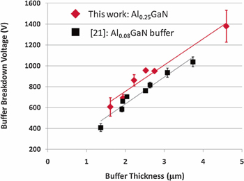 Figure 1: Buffer breakdown voltage versus total layer thickness. The comparison with the paper’s ref. [21] is with previous IMEC/Katholieke Universiteit Leuven work published in 2009.
With 200nm-thick intermediate layers (samples A1–4), the material quality indicated by x-ray diffraction rocking curves (sample A4) is comparable with previous results on smaller 4-inch diameter silicon wafers and the best values in the literature. Samples B with thicker intermediate layers were tested with thicker buffer layers, as needed for high breakdown voltage (Figure 1). While sample B2 had the highest breakdown voltage at 1380V, it also has a large concave bowing parameter. Positive bow indicates convex surfaces.
 The DHFET material was also tested for mobility and carrier concentration of the two-dimensional electron gas (2DEG) of the channel, using van der Pauw Hall measurements. The average electron mobility was ~1766cm2/V-s and the carrier concentration 1.16x10¹³/cm2. These values result in a low sheet resistance of 306Ω/sq. “These values even outperform the ones obtained on 150mm silicon substrates,” the researchers write.
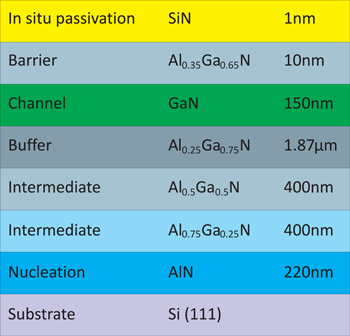
Figure 2: DHFET structure.
DHFETs (Figure 2) were produced based on buffers grown as for sample B1, which has a breakdown voltage above 950V. After the buffer, a 150nm GaN channel and a 10nm Al0.35Ga0.65N barrier were grown. Finally, a Si3N4 layer was grown to stabilize and passivate the Al0.35Ga0.65N surface. Processed devices delivered currents up to 0.65A/mm. “More detailed device results will be published elsewhere,” the team promises.
The paper concludes: “GaN-based power devices grown on 200mm Si substrates show great potential for integrating GaN processing on a standard silicon technology platform.”
IMEC AMAT DHFETs MOCVD GaN AlGaN
http://apex.jsap.jp/link?APEX/5/011002
The author Mike Cooke is a freelance technology journalist who has worked in the semiconductor and advanced technology sectors since 1997.