- News
5 January 2012
China creates its first high-performance InAlN HEMTs on sapphire
Hebei Semiconductor Research Institute and Harbin Institute of Technology researchers have made the first report in mainland China of high-performance high-electron-mobility transistors (HEMTs) using indium aluminum nitride (InAlN) barriers on gallium nitride (GaN) buffer layers [Liu Bo et al, J. Semicond., vol32, p124003, 2011]. The team sees their work as strengthening the case for InAlN-based technology as a potential successor of aluminum gallium nitride (AlGaN) HEMTs for microwave and millimeter-wave power applications
Growth of high-quality InAlN has only recently become available. Potential advantages of InAlN over the more traditional AlGaN include lattice matching with GaN with In-content of ~17% and high spontaneous polarization that creates high charge carrier densities in the two-dimensional electron gas (2DEG) that forms at InAlN/GaN interfaces. These properties allow the gate–channel distance to be reduced, improving electrostatic control of current flow through the device.
Usually AlGaN/GaN HEMT channel–gate distances are 25nm. The Hebei/Harbin InAlN/AlN/GaN devices had almost half that at 13nm. For example, the new devices had peak transconductance of 286mS/mm at gate potential of –3V. With sub-100nm gate lengths, the researchers expect to achieve transconductances of more than 400mS/mm, along with low output conductance and high gain at mm-wave frequencies.
 Although the Hebei/Harbin InAlN/AlN/GaN device had modest frequency performance with extrinsic fT cut-off of 34GHz and fmax maximum oscillation of 40GHz at a gate potential –4V and a drain bias of 8V, researchers based in Switzerland have recently achieved 205GHz cut-off with 55nm gate length and 3nm InAlN barrier layer.
Power measurements of Hebei/Harbin device subjected to a drain voltage of 24V in a load-pull system at 10GHz gave output power density of 4.69W/mm, linear gain of 11.8dB, and peak power-added efficiency (PAE) of 48%. The power density figure compares with AlGaN/GaN device performance of 41.4W/mm at 4GHz and 3.65W/mm at 18GHz.
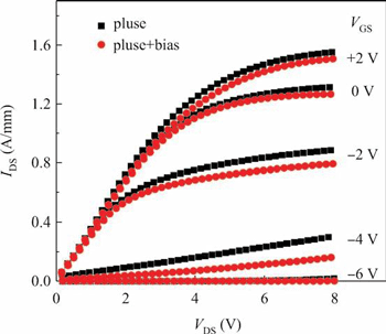
The maximum drain current density for the Hebei/Harbin device was 1.56A/mm at a gate potential of +2V, a value “to our knowledge beyond the highest drain current density of any AlGaN/GaN HEMT structure, especially for samples fabricated on sapphire substrates,” the researchers add. Higher current densities are expected from improved thermal management and reduced trap densities.
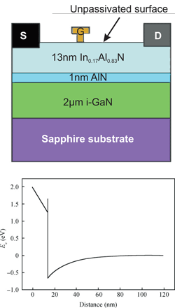
The devices (Figure 1) were grown on sapphire using low-pressure metal-organic chemical vapor deposition (LP-MOCVD). The In-content of ~17% was measured on a 100nm InAlN layer sample using x-ray diffraction techniques. Then a 13nm InAlN layer sample was grown for the production of HEMTs.
Figure 1: Structure and energy band diagram of a schematic InAlN/GaN HEMT.
The ohmic source–drain contacts were titanium/aluminum/nickel/gold and the Schottky gate was nickel/gold. The source–drain electrodes were subjected to a rapid thermal anneal at 850°C for 30s in nitrogen. The source–drain contacts had resistances of 0.6Ω-mm. The gate length was 0.25μ. The gate width was 2x100μm.
 Hall measurements of the performance of the two-dimensional electron gas at the InAlN/AlN/GaN interface gave a mobility of 1210cm2/V-s with a carrier concentration of 2.6x10¹³/cm2. The sheet resistance was 210Ω/sq. The sheet carrier density was about twice that typical for AlGaN/GaN interfaces. The researchers attribute their high performance values to the optimized nature of their AlN and InAlN layers.
Unpassivated devices showed almost current-collapse-free performance with pulsed operation (Figure 2). AlGaN/GaN-based devices tend to suffer from surface charging effects from trap states that cause the current response to decrease when the gate and drain potentials are pulsed.
Figure 2: Pulse DC characteristics of unpassivated InAlN/ GaN HEMT.
The researchers comment on their results: “A much lower current dispersion was observed in our case, although these devices were still unpassivated, indicating a relatively stable surface in the case of the AlInN barrier material.”
Increasing power density for InAlN/GaN HEMTs on sapphire
InAlN HEMTs on sapphire InAlN/GaN HEMTs Sapphire substrates
The author Mike Cooke is a freelance technology journalist who has worked in the semiconductor and advanced technology sectors since 1997.
