- News
13 January 2012
Growth-mode transition to higher UV output
Researchers in Taiwan have used a heavily silicon-doped layer to improve the performance of ultraviolet light-emitting diodes (LEDs) [Shih-Cheng Huang et al, J. Appl. Phys., vol110, p123102, 2011]. The silicon doping created a growth-mode transition layer (GMTL) that was designed to bend or stop threading dislocations (TDs) in the nitride semiconductor material from affecting light emission.
It is thought that the incorporation of silicon in the undoped gallium nitride (GaN) partially relaxes residual stress arising from the large lattice mismatch with the sapphire substrate. The researchers also believe that the GMTL transforms the growth from a ‘two-dimensional’ (2D) layer-by-layer mode to a 3D ‘island’ mechanism. In the latter mode, the TDs are reduced by growth that bends their orientation into a lateral direction.
The LEDs were grown on 2-inch c-plane sapphire using metal-organic chemical vapor deposition (MOCVD). The layers were designed for the emission of 375nm ultraviolet light (Figure 1). Aluminum gallium nitride (AlGaN) grown on a GMTL had TD densities reduced by an order of magnitude compared with layers grown without the GMTL; the density values were 8x10⁷/cm2 and 8x10⁸/cm2, respectively.
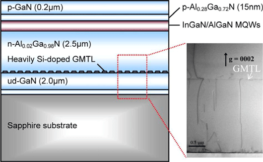
Figure 1: Schematic structure of UV-LEDs. Inset: TEM images show the effect of GMTL on threading dislocations. The multi-quantum well layer consisted of a ten-period structure with 3nm indium gallium nitride (3% indium) wells and 11nm aluminum gallium nitride (6% aluminum) barriers. A 30nm GaN buffer was grown before the undoped 2μm GaN layer. The GMTL was 50nm thick.
X-ray diffraction peaks also narrowed with GMTL material, indicating improved crystalline quality: the peak arising from the (002) plane was 270 arcsec with GMTL and 360arcsec without; and from the (102) plane the values were 380 arcsec and 460 arcsec, respectively.
For electroluminescence testing up to 1A (Figure 2), the devices were gold wire-bonded and packaged into TO-66 epoxy-free metal cans. At 350mA, the output powers were 286.7mW and 204.2mW for the GMTL and conventional devices, respectively, representing a 40.4% enhancement for the new device structure.
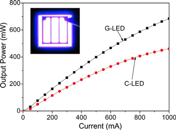 Figure 2: LED output power vs injection current for GMTL and conventional LEDs. Inset: photograph of GMTL LED at 350mA injection.
The researchers see applications for UV-LEDs coming from sensing, curing, and photocatalysis. Also, there is potential for white light with better color-rendering indices than the present blue-LED-pumped YAG-phosphor combination.
The research team consisted of participants from National Chung Hsing University, National Chiao-Tung University, Chung Yuan Christian University, Da-Yeh University, Advanced Optoelectronic Technology Inc., and National Cheng Kung University.
The internal quantum efficiency (IQE) of the epitaxial material structures was assessed through photoluminescence (PL) measurements at low temperature (20K) and room temperature. The dependence of the IQE values varied with excitation carrier density. The peak IQE value was assumed to be 100% at 20K. This peak occurred around 1016/cm3.
The researchers describe the decrease in IQE at 20K beyond the peak as being similar to the droop phenomenon that reduces the external quantum efficiency of visible LEDs at high current injection. The researchers comment: “According to our experimental data, we infer that the low-temperature IQE decrease at high excitation carrier density is due to the carrier overflow and dislocation density.”
Spectral measurements of PL intensity at 20K give a main peak at 375nm and a shoulder at 380nm at higher excited carrier densities that is attributed to overflow into the p-AlGaN layer. At room temperature, there is no shoulder. Although the electroluminescence peaks are no doubt in this region, the presence of electric fields and free charge carriers tends to shift the emission wavelength as the current changes.
The room temperature IQE of the LED with GMTL was enhanced by 40.6% over that of the conventional device. The peak IQE occurred at higher carriers densities beyond 1017/cm3. The peak IQE of the GMTL device was around 45%.
Electrically, the reverse current is reduced by the presence of the GMTL layer to 0.005μA at 5V, compared with 0.048μA for the conventional LED. This also indicated improved material quality.
http://link.aip.org/link/doi/10.1063/1.3669377
The author Mike Cooke is a freelance technology journalist who has worked in the semiconductor and advanced technology sectors since 1997.