- News
20 January 2012
Aluminum oxide passivation reduces off-current in AlN/GaN transistors
Hong Kong University of Science and Technology has used aluminum oxide (Al2O3) gate dielectric and passivation on aluminum nitride/gallium nitride (AlN/GaN) transistors to reduce off-state leakage currents by almost four orders of magnitude [Tongde Huang et al, IEEE Electron Device Letters, published online 27 December 2011].
High-quality AlN/GaN structures have only recently become available in metal-organic chemical vapor deposited form (as opposed to that from molecular beam epitaxy). Their advantage lies in the material polarization contrast between AlN and GaN offering higher two-dimensional electron gas densities (2DEGs) than AlGaN/GaN or InAlN/GaN. In addition, researchers have been able to grow AlN/GaN on silicon substrates, promising lower-cost products.
In comparison with Schottky heterostructure field-effect transistors (HFETs, i.e. without gate insulation), the off-state drain current leakage was reduced in the metal-oxide-semiconductor HFET (MOSHFET) by almost four orders of magnitude from 2.5x10⁻¹mA/mm (HFET) to 7.6x10⁻⁵mA/mm (MOSHFET) at 6V drain bias. This increased the on/off current ratio (Ion/Ioff) to 108 (measured at gate potentials of +2V and –5V, respectively). The maximum drain current and peak transconductance were 745mA/mm and 280mS/mm, respectively.
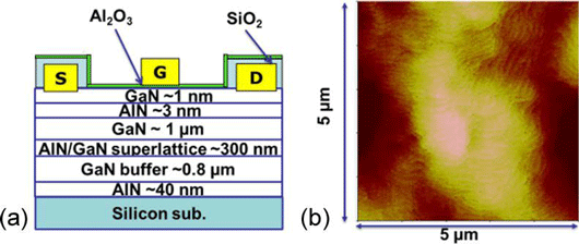
Figure 1: Cross-sectional schematic of the AlN/GaN MOSHFETs (a), and AFM image of AlN surface (b).
The nitride semiconductor heterostructure for the MOSHFET was grown on (111) silicon using metal-organic chemical vapor deposition (Figure 1). The superlattice interlayer, designed to relax strain in the structure, consisted of some 9 periods of alternate layers of 6nm of AlN and 28nm Al0.19Ga0.81N to make 300nm. Room-temperature Hall measurements gave a mobility of 1050cm2/V-s and an electron density of 1.44x10¹³/cm2. These factors combine into a sheet resistance of 415Ω/sq.
The MOSHFETs were processed by beginning with etch of the isolation mesa and deposition and annealing of titanium/aluminum/nickel/gold source–drain electrodes. The annealing was at 850°C and gave contact resistance values of 0.34Ω-mm and a specific contact resistance of 3.7x10⁻⁶Ω-cm2. The surface was covered with silicon dioxide to protect the atomic layer deposition (ALD) chamber from metal contamination during the growth of the amorphous aluminum oxide dielectric layer. The silicon dioxide in the active gate region was removed before the aluminum oxide deposition.
Finally the gate electrode (consisting of nickel/gold) was deposited. The gate length was 1μm and the gate–source spacing was also 1μm.
The aluminum oxide passivation layer is seen as an essential component of AlN/GaN devices since the thinness of the AlN layer makes the 2DEG channel particularly sensitive to surface states. Devices produced without aluminum oxide passivation suffered from current and transconductance degradation during repeated sweeps of the gate-voltage characteristics with drain bias of 6V. Eventually, the drain current and transconductance were not measurable. The effect is due to electrons being trapped in the surface states, but not being released in time to restore the device performance. This negative charge depletes the 2DEG cutting off drain current flow.
The researchers report: “We found that this degradation phenomenon could be completely eliminated by adding an Al2O3 passivation layer on the transistor surface.”
In addition, the aluminum oxide insulates the gate electrode. The researchers also tested transistors with silicon nitride passivation, which has also been found effective in eliminating current degradation.
Comparisons between aluminum oxide and silicon nitride passivation showed increased current with thicker Al2O3 layers, the enhancement saturating around 15nm thickness. With 7nm aluminum oxide, the current was higher than that given by 15nm silicon nitride. The researchers conclude that Al2O3 is a better candidate for passivation than SiNx.
Direct current characteristics were also compared with 500μsec pulses applied to the gate of Al2O3 passivated devices once a second from a –4V base condition where the device is pinched off. The current is only slightly lower in the pulsed measurements at low drain bias. At higher biases, the current was actually higher than the DC condition, likely due to self-heating during measurement releasing charge from the trap states. By contrast, unpassivated devices suffer from significantly reduced current in pulsed operation. Another advantage of the passivation is more uniform performance between devices.
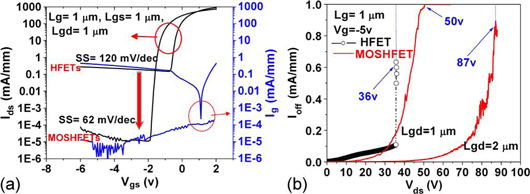
Figure 2: (a) Semilog transfer curves of drain current and gate leakage current in HFETs and MOSHFETs. (b) Breakdown voltage curves of HFETs with gate–drain distance (Lgd) of 1μm and MOSHFETs with distances of 1μm and 2μm.
The effect of Al2O3 layer thickness on the 2DEG Hall measurements was an increase in electron density above 7nm to almost 3x10¹³/cm2. However, the mobility was reduced to around 600cm2/V-s. The combined effect was a slight reduction in sheet resistance.
The researchers explain these results: “The proposed mechanism for the increased 2DEG density is the positive charges in the dielectric/semiconductor interface and stress due to the deposited Al2O3. The mobility drop after Al2O3 passivation may be a result of increased scattering among interfacial charges and electrons.”
Perhaps one of the most impressive results was a sub-threshold slope of 62mV/dec, which is close to the theoretical limit for planar MOSHFET structures at room temperature (300K). By contrast, the Schottky gate device had a sub-threshold value of 120mV/dec. The researchers comment: “The improved SS obviously is also due to the large Ion/Ioff ratio in the MOSHFETs.”
The MOSHFET also had improved breakdown characteristics. With a gate–drain distance of 1μm, the breakdown at gate potential of –5V (BVoff) was 36V for the HFET and 50V for the MOSHFET. Increasing the gate–drain distance improved the MOSHFET breakdown to 87V.
First e-mode AlInN/GaN MOS-HFET using SiON insulation
Aluminum oxide passivation AlN/GaN transistors
The author Mike Cooke is a freelance technology journalist who has worked in the semiconductor and advanced technology sectors since 1997.