- News
11 July 2012
LayTec enlarges sales team; training center opened at Taiwan’s Challentech
 LayTec AG of Berlin, Germany (which makes in-situ metrology systems for thin-film processes, focusing on compound semiconductor and photovoltaic applications) says that on 21 June Challentech International Corp, its partner for sales and service in Taiwan, opened its new training center in Hsinchu. LayTec’s president & founder Thomas Zettler and general manager of sales Tom Thieme attended the opening ceremony.
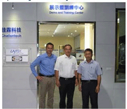
Picture: Tom Thieme (general manager sales at LayTec), Thomas Zettler (CEO & president of LayTec), and C.M. Liu (president of Challentech International) in front of the new training center.
At the training center, tools such as the EpiCurve TT AR Blue and the first PreCurve, LayTec’s new product for ex-situ measurement of wafer-bow before and after epitaxial growth, are demonstrated and used for training purposes.
 Also, LayTec has appointed Stephanie Fritze as a new sales team member, supporting activities in Taiwan and China. Fritze obtained her diploma in physics at the Otto-von-Guericke-Universität in Magdeburg on x-ray diffraction and fluorescence analysis of nitride semiconductors. Her PhD research topic was gallium nitride on silicon (GaN-on-Si) epitaxy and characterization, with a special focus on GaN-based LED growth on large-diameter substrates. She was also involved in the construction and start-up of a lithography laboratory for conventional and thin-film LED processing. Fritze has broad knowledge of the growing field of GaN-on-Si applications, says LayTec.
Picture (right): New sales team member, Stephanie Fritze.
 In addition, Emilie Quillet has joined LayTec’s sales force to support business in Europe. She obtained her engineering degree in materials science at the University of Technology of Troyes (France) and did her M.Sc. thesis at Helsinki University Technology (now Aalto University), where she studied the influence of plasmonic coupling on light extraction of InGaN/GaN SQW-based GaN LEDs. Afterwards, as a sales engineer for LED lighting at Ekolicht MMK GmbH, she gained experience in product integration, customer networking and relationship management.
Picture (right): New sales team member, Emilie Quillet.
![]() Finally, new sales team member Volker Blank will focus predominantly on supporting activities in South Korea. He received his Diploma in Physics from Johann Wolfgang Goethe-University of Frankfurt-am-Main for studying photo-induced charge carriers in organic semiconductors by time-resolved terahertz-spectroscopy. For his PhD he worked on broadband terahertz radiation from optically driven air plasmas, targeting ultra-broadband THz pulses for spectroscopic applications.
Finally, new sales team member Volker Blank will focus predominantly on supporting activities in South Korea. He received his Diploma in Physics from Johann Wolfgang Goethe-University of Frankfurt-am-Main for studying photo-induced charge carriers in organic semiconductors by time-resolved terahertz-spectroscopy. For his PhD he worked on broadband terahertz radiation from optically driven air plasmas, targeting ultra-broadband THz pulses for spectroscopic applications.
Picture (right): New sales team member, Volker Blank.
LayTec orders
LayTec says that it has received a repeat order from Jenoptik in Berlin, Germany. At Jenoptik, LayTec´s EpiTT sensors are used on Aixtron G3 metal-organic chemical vapour deposition (MOCVD) systems for monitoring the growth of AlGaAs-based laser structures. Dr Martin Zorn, senior scientist at Jenoptik‘s Lasers & Material Processing division, says that, by using EpiTT, he has been able to optimize the laser emission wavelength and growth rate homogeneity. The EpiTT sensors enable in-situ determination of wafer temperature and growth rate of each individual layer on every wafer.
LayTec has also installed its first metrology system in India. The latest member of EpiCurveTT series, the EpiCurveTT SP (Single Port), is now being used on an Aixtron 3x2” CCS MOCVD system at Tata Institute of Fundamental Research (TIFR) in Mumbai, India.
Also, two research groups focusing on GaN epitaxial crystal growth at the University of Tokyo and the University of Meijo have chosen LayTec in-situ sensors for their Aixtron AIX200/4 RF-S and Taiyo Nippon Sanso SR-4000 MOCVD systems, respectively.
LayTec notes that, due to expansion in the market for power device using GaN-on-Si and SiC, strong demand for in-situ curvature measurement is being seen in Japan. Since there is a large mismatch in the thermal expansion coefficients of GaN and silicon, strain engineering during growth is necessary. Also, wafer size has recently been migrating from small size to large size (6“ and 8“), so strain engineering using the EpiCurve TT series is becoming even more important, the firm adds.