- News
17 July 2012
Ballistic deflection with improved transconductance using aluminium oxide
University of Massachusetts Lowell, Universidad de Salamanca, and North Carolina State University have integrated aluminium oxide dielectric into III-V ballistic deflection transistors (BDTs) for the first time [Vikas Kaushal et al, IEEE Electron Device Letters, published online 3 July 2012]. The effect of the dielectric is to increase transconductance (by about 2x) and to shift the transconductance peaks to lower biases.
Room-temperature BDTs have positive and negative transconductance regions that enable the design of inverting or non-inverting circuits, depending only on the gate offset voltage. The non-linear transfer function of such devices could be used to perform frequency doubling up 400GHz at room temperature, according to simulations.
The researchers have incorporated high-k aluminium oxide (Al2O3) dielectric with the aim of improving the electrostatic gate–channel coupling through the dielectric trenches.
Ballistic transport is achieved through reducing device dimensions to the order of the carrier mean free path, i.e. ~200nm for two-dimensional electron gases (2DEGs) in indium gallium arsenide (InGaAs) at room temperature. Short mean-free paths (compared with device dimensions) give traditional ohmic/viscous resistivity. The long mean-free path of ballistic devices opens up new charge carrier behaviors that could lead to future high-performance logic and analog applications.
The BDT fabrication was performed at the Center for Nanoscale Systems at Harvard University. The epitaxial material consists of lattice-matched layers of InGaAs and InAlAs on indium phosphide (InP) substrate: 450nm InAlAs buffer, 50nm InGaAs channel, 20nm InAlAs spacer, silicon δ-doped InAlAs, and 10nm InGaAs cap. The structure creates the conditions for a two-dimensional electron gas (2DEG) with sheet electron carrier density of 1012/cm2 and mobility of 1.1x104cm2/V-s.
The six-terminal planar structure of the BDT (Figure 1) was formed with electron-beam lithography (EBL), inductively coupled plasma–reactive-ion etching (ICP-RIE) to make a mesa with 130nm step height, further EBL to allow selective deposition of nickel-germanium-gold contacts (annealed at 420°C for 30 seconds), and finally titanium-gold contact pads were applied in a lift-off process. Two basic BDT types were produced: one with a channel width of 140nm and the other with a channel width of 200nm.
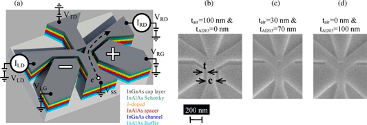
Figure 1: (a) Three-dimensional ‘artistic’ topology and heterostructure of typical BDT. Top-left and top-right contacts are drain terminals; bottom-left and bottom-right terminals are gates; top contact is a bias terminal that controls gain, and the bottom terminal the source. (Inset) Schematic showing electron trajectory for positive right gate bias condition (VRG = –VLG). SEM image (with scale indicator) of top view of BDT with a channel width of 140nm and a trench width (b) of 100nm air; (c) 70nm Al2O3, 30nm air; and, (d) 100nm Al2O3.
The in-plane BDT terminals – grounded source, three drains (left, right and top), and left and right gates – provide control of carrier density and transport direction. Aluminium oxide dielectric was deposited using 200°C atomic-layer deposition (ALD), filling the gap between the gates and channel.
 The effect of filling the trenches with aluminium oxide is to create surface states at the oxide–semiconductor interface and to increase gate–channel coupling. Surface states degrade mobility and deplete the carrier density in the channel. Increased gate–channel coupling creates early pinch-off. Both these factors tend to reduce the channel current.
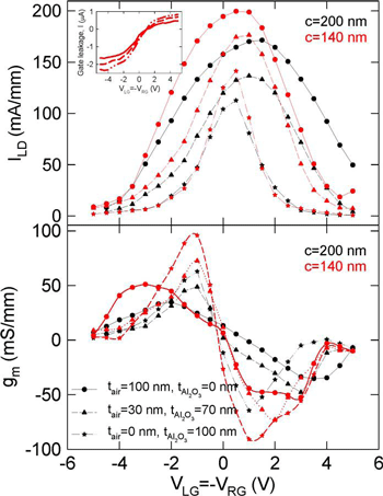
Figure 2: (a) Transfer characteristics and (b) transconductance of BDT normalized to channel widths of 200nm and 140nm. Depositing 35nm and 50nm of Al2O3 along both walls of trench resulted in 70nm and 100nm of net effective Al2O3 in trenches. The three drain terminals were biased at 1V. The inset in (a) shows gate leakage current for BDT 140nm channel width.
For example, in a 140nm-wide channel device the current is decreased by 29% by filling the trenches with 100nm of Al2O3 (Figure 2). At the same time, the transconductance peaks (positive and negative) shift in from about +/–3V to +/–1V and also double in value. The 140nm device has higher current density, has earlier pinch-off, and a slight increase in transconductance, compared with the 200nm device.
The author Mike Cooke is a freelance technology journalist who has worked in the semiconductor and advanced technology sectors since 1997.