- News
20 June 2012
First 40GHz 2.5W/mm output performance of GaN/Si HEMTs
Institute for Electronics, Microelectronics and Nanotechnology (IEMN) in France has demonstrated high-power-density nitride high-electron-mobility transistors (HEMTs) on silicon (Si) at 40GHz “for the first time” [F. Medjdoub et al, IEEE Electron Device Letters, published online 14 June 2012]. Devices based on aluminium gallium nitride (AlGaN) layers on Si have previously demonstrated high power performance up to 26.5GHz.
The IEMN devices use AlN top barriers rather than the more usual AlGaN. The new HEMTs also incorporate an AlGaN back-barrier to reduce subthreshold drain leakage current and short-channel effects. The 40GHz performance brings Ka-band (26.5−40GHz) applications into range, such as satellite communications, high-resolution, close-range targeting radars for military aircraft, and remote vehicle speed measurement (speed traps).
The researchers comment: “These results show that an AlN/GaN/AlGaN heterostructure grown on silicon substrate is a viable technology for cost-effective high-power millimeter-wave amplifiers fully compatible with standard Si-based devices.”
Nitride HEMTs on Si have previously been proposed for lower-frequency power applications such as DC–DC converters, where one attraction is the lower cost from using large-diameter silicon substrates (up to 8-inch/200mm at present). If RF GaN-on-Si HEMTs could be combined with well-established Si-based technologies, new chips with higher functionalities and performance might become possible.
IEMN worked with AlN/GaN/AlGaN double-heterostructure epitaxial material supplied by EpiGaN nv of Hasselt, Belgium (which was spun off from nanoelectronics research center Imec of Leuven, Belgium in 2010). The material was grown using metal-organic chemical vapor deposition (MOCVD) on high-resistance 4-inch Si substrates.
A silicon nitride (SiN) cap was grown in-situ (i.e. in the MOCVD process chamber) at EpiGaN with the aim of providing early passivation and preventing strain relaxation of the structure. The strain increases the polarization contrast that is used to create the two-dimensional electron gas (2DEG) channel that forms near the AlN/GaN interface. The resulting higher-density 2DEG allows thinner top barrier layers, which brings the gate closer to the channel, improving electrostatic control.
Hall measurements of the material gave a carrier concentration of 2.1x10¹³/cm2 and a carrier mobility of 1400cm2/V-s. The resulting sheet resistance was 240Ω/square.
Source, drain and gate contacts were added (Figure 1) along with further SiN. The 0.1μm-long nickel-gold T-gate included a field-plate with 0.2μm extension toward the drain. The gate−source spacing was 0.3μm. The gate−drain spacing was 2μm. The device width was 50μm. A final passivation layer of 150nm SiN was then applied.
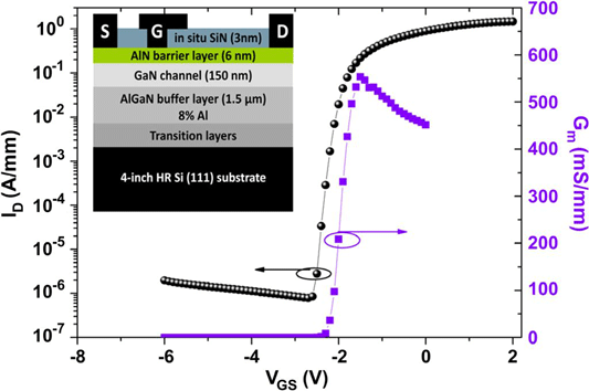
Figure 1: Transfer characteristics at 6V drain bias of IEMN HEMT. Inset: schematic cross-section of fabricated HEMT.
The maximum drain current at +2V gate potential was 1.8A/mm, and the off-state leakage was less than 2μA/mm. Three-terminal breakdown defined by 1mA/mm leakage was more than 100V. The extrinsic transconductance peaked at 550mS/mm. Pulsed measurements showed almost no gate lag, but there was a slight drain lag.
Frequency performance was measured over the range up to 50GHz. The maximum oscillation frequency (fmax) was 200GHz; the current-gain cut-off (fT) was 80GHz. Continuous wave (CW) output power at 40GHz was measured using an active load-pull large-signal network analyzer (LSNA).
The researchers comment: “An output power density of 2.5W/mm was reached at 40GHz when biased at 15V, which represents, to our knowledge, the first demonstration of high power density at 40GHz for a GaN-on-Si transistor (as shown in the inset in Fig. 2).”
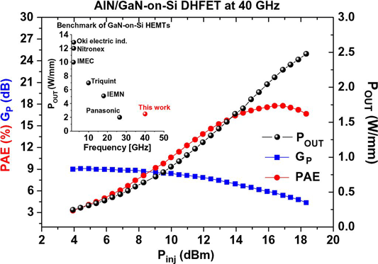
Figure 2: CW power sweep at 40GHz of AlN/GaN/AlGaN HEMT on highly resistive silicon substrate at drain bias of 15V and gate potential of −1.6V. Inset: RF power density benchmark of GaN-on-Si transistors.
The power-added efficiency (PAE) peaked at 18% and the linear gain was 9dB. The limiting factors for the PAE are given as self-heating and parasitic conduction at the buffer/silicon interface.
The researchers comment that performance at drain bias beyond 15V is limited by thermal effects. Their on-going work aims to optimize the Al content of the buffer to improve thermal dissipation, along with improving the buffer/Si interface quality to enhance large-signal gain at millimeter-wave frequencies. Thermal performance could also be enhanced by back-side processing through substrate thinning and application of a heat-sink.
http://ieeexplore.ieee.org/xpl/articleDetails.jsp?arnumber=6218165
The author Mike Cooke is a freelance technology journalist who has worked in the semiconductor and advanced technology sectors since 1997.