- News
15 June 2012
PVcomB starts production of 30cm x 30cm thin-film PV modules
 The Berlin Competence Centre for Thin Film and Nanotechnology for Photovoltaics (PVcomB) – a joint initiative of the Helmholtz Centre Berlin for Materials and Energy (HZB) and the Technical University of Berlin – has started operation of two thin-film solar-module production tools together with their supplier Leybold Optics GmbH of Alzenau, Germany.
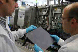
Picture: From right to left: Dr Bernd Stannowski and Dr Sven Ring of PVcomB. (Photo: HZB.)
PVcomB says that, with the inline sputter systems from Leybold Optics, it has closed the final gaps in its two research lines for thin-film silicon and copper indium gallium diselenide (CIGS) solar modules, and has now started full operation of modules measuring 30cm x 30cm.
Summing up PVcomB’s mission, its head Dr Rutger Schlatmann cites “continuous thin-film technology developments in the laboratory, which must be implemented on an industrial level as quickly as possible”. In particular, scientists and technicians work on the two research lines, focussing on the needs of industry, with the aim of solving problems related to industrial production. At the same time, alternatives arising out of basic research are developed and tested at each process and analysis stage.
The Leybold Optics sputter systems were finally commissioned in May, completing the research lines. PVcomB is now able to perform the entire module production process, from cleaning the glass panels all the way to module encapsulation, for a glass panel size of 30cm x 30cm.
The first A600V7 sputter system is part of the reference line for thin-film silicon (a-Si/μc-Si), enabling PVcomB to now produce its own layers for front and back contact systems. The second A600V7 plays a key role in the reference line for CIGS. Back contacts made of molybdenum and, above all, the layers consisting of copper, gallium and indium are deposited in the ‘sequential process’. In the subsequent steps, these are transformed into the CIGS modules.
PVcomB says that the technology of the A600V7 inline sputter system, together with Leybold Optics’ experience in coating solutions for PV applications, were decisive factors when it came to modifying its research lines for the technically complex sputter processes. Moreover, the Leybold Optics systems have great flexibility, allowing subsequent integration of additional components and system extensions. The use of carrier stackers for changing substrates and the ability to coat two substrates simultaneously means that automated processes can be run with high throughput and a high level of reproducibility.
“Our inline sputter systems enable us to fulfil PVcomB’s stringent requirements of producing CIGS and thin-film silicon solar modules in a state-of-the-art environment,” says Patrick Binkowska, manager of the Glass & Solar Division at Leybold Optics. “At the same time, this cooperation has afforded us a wonderful opportunity to learn from the experience of the PVcomB research team,” he adds. “The resulting findings flow into our ongoing development process for the next system generation.”
www.helmholtz-berlin.de/projects/pvcomb