- News
7 June 2012
Gold-free nitride MOS-HEMTs for CMOS compatibility
Singapore and Hong Kong researchers have developed a gold-free CMOS-compatible process for nitride semiconductor metal–oxide–semiconductor high-electron-mobility transistors (MOS-HEMTs) [Xinke Liu et al, Appl. Phys. Express, vol5, p066501, 2012]. The participating institutions were National University of Singapore, Hong Kong University of Science and Technology, and Singapore’s Nanyang Technological University.
Aluminium gallium nitride (AlGaN) alloys have a wide bandgap that makes them attractive for high-power/voltage operation, allowing the development of switches for boost converters, power factor correction (PFC) circuits, uninterruptable power supplies (UPS), etc. The development of AlGaN/GaN HEMTs on silicon promises the merging of nitride technology with mainstream CMOS circuitry, along with production cost reductions from the larger-diameter silicon wafers (150mm, 200mm) that are available.
However, to enable mixed nitride/silicon semiconductor technology, CMOS-compatible processes need to be developed. One issue is the general use of gold in nitride semiconductor transistor contacts. Gold reduces carrier lifetimes in silicon; although this may be desired in some applications such as infrared detection, it is to be avoided at all costs in CMOS circuits.
The epitaxial material for the Singapore/Hong Kong devices (Figure 1) was grown using metal-organic chemical vapor deposition (MOCVD) on 4-inch p-silicon (111) wafers. The 3.3μm buffer region consisted of multiple pairs of AlN and GaN layers. The device layers consisted of 1.5μm GaN followed by 25nm Al0.25Ga0.75N barrier.
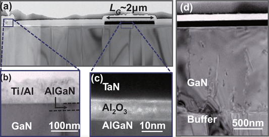
Figure 1: (a) Cross-sectional TEM image of fabricated gold-free AlGaN/GaN MOS-HEMT. (b) Zoomed-in image of a Ti/Al contact on AlGaN layer. (c) Zoomed-in image of a TaN/Al2O3/AlGaN stack. (d) Cross-sectional TEM image of TaN/Al2O3/AlGaN/GaN/buffer.
Mesas for device isolation were formed using chlorine plasma reactive ion etch (RIE), followed by native oxide removal and passivation in ammonium sulfate ((NH4)2S) solution. Aluminium oxide
(Al2O3) gate dielectric was applied using atomic layer deposition (ALD), followed by a 450°C anneal in nitrogen for 60 seconds.
The 2μm-long gate electrode consisted of sputtered tantalum nitride that was subsequently patterned and etched in chlorine plasma that was selective against the aluminium oxide gate dielectric as etch stop. The etch process was CMOS compatible.
The devices were then encapsulated in silicon dioxide. Contact openings were patterned and etched. Aluminium/titanium (71nm/30nm) stacks were used for source-drain metals, with ohmic contact created through alloying at 650°C for 30 seconds in nitrogen. The source–gate and drain–gate distance were both 5μm.
The threshold voltage of one resulting device was -6.3V, the negative value indicating normally-on (depletion-mode) behavior. The subthreshold swing was 90mV/dec and the peak transconductance was 41.6mS/mm with 5V drain bias.
On average, the subtheshold swing was 97.7mV/dec, the on–off current ratio was 106, and the gate leakage was 1.02x10⁻⁶A/mm. Variations in performance were attributed to differences in interface trap density at the Al2O3–AlGaN interface and the thickness of the AlGaN barrier layer. The on-resistance was around 3mΩ-cm2.
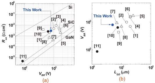
Figure 2: (a) Breakdown voltage VBR versus on-resistance Ron of fabricated AlGaN/GaN MOS-HEMTs, compared with those of state-of-the-art AlGaN/GaN MOS-HEMTs. (b) Breakdown voltage VBR versus gate-to-drain spacing LGD of fabricated AlGaN/GaN MOS-HEMTs, compared with those of state-of-the-art AlGaN/GaN MOS-HEMTs. Open symbol: GaN MOS-HEMTs with gold. Solid symbol: GaN MOS-HEMTs without gold. Square: GaN-on-sapphire. Triangle: GaN-on-SiC. Circle: GaN-on-silicon.
A vertical breakdown voltage of more than 800V was suggested by four-terminal off-state measurements with the gate bias at -12V and drain voltage kept to less than 1mA/mm. At 650V drain bias, the off-current was 3.8x10⁻⁷A/mm. At 800V, the substrate current was around 10-7A/mm.
The researchers comment that the 800V breakdown “is the highest for LGD below 10μm for AlGaN/GaN/Si MOS-HEMTs fabricated using a gold-free process.”
The researchers conclude: “A gold-free process enables the fabrication of GaN power devices in Si foundries without the risk of contamination. The devices could be generally useful for cost-competitive power switching circuits with a supply voltage in the range of several hundred volts.”
http://apex.jsap.jp/link?APEX/5/066501
The author Mike Cooke is a freelance technology journalist who has worked in the semiconductor and advanced technology sectors since 1997.