- News
19 March 2012
University of Texas at Austin demonstrates high-quality wafer-scale graphene using Aixtron system
Researchers at the University of Texas at Austin, USA have demonstrated high-quality wafer-scale deposition of graphene on evaporated copper films for the first time, using their recently acquired cold-wall vertical BM (Black Magic) Pro reactor from deposition equipment maker Aixtron SE of Herzogenrath, Germany (Li Tao et al, ‘Synthesis of High Quality Monolayer Graphene at Reduced Temperature on Hydrogen-Enriched Evaporated Copper (111) Films’, ACS Nano (2012), DOI: 10.1021/nn205068n).
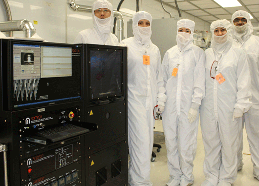
Picture: The Aixtron BM Pro PECVD reactor, with members of Akinwande’s group - (left to right): Li Tao (postdoc scholar), Nassibe Rahimi, Kristen Parrish, Maryam Mortazavi and Fahad Chowdhury (all PhD students).
“Most research and synthesis of graphene to date has been on copper foil, and while good-quality films can be achieved using such a method, we have succeeded in depositing monolayer graphene chemical with negligible defects onto evaporated copper films on the wafer-scale,” says professor Deji Akinwande, who led the research together with professor Rod Ruoff’s team at the Microelectronics Research Center at UT Austin. “A pre-annealing process is used at first to create a hydrogen-rich polycrystalline copper film of <111> preferential orientation, followed by the decomposition of pure methane for the growth of high-quality grapheme. The growth proceeds without the need for hydrogen gas during the growth phase, and occurs at a lower processing temperature than on copper foil,” he adds.
“This work creates a pathway for wafer-scale synthesis of graphene with negligible defects, which is an essential requirement for heterogeneous graphene/Si VLSI applications and industrial adoption of grapheme,” says Akinwande. “Indeed, the BM Pro is a high-performance, flexible platform with unique chemical vapor deposition (CVD) processing capabilities,” he adds. “This allowed us to conduct our research effectively and achieve these growth results in a short time with outstanding uniformity on the wafer-scale.”
The experimental work was carried out at the National Nanotechnology Infrastructure Network (NNIN) and Texas Materials Institute (TMI) facilities at The University of Texas at Austin and is supported in part by the Nanoelectronic Research Initiative (NRI-SWAN Center), and the Office of Naval Research. Established in 1983, the Microelectronics Research Center is equipped with semiconductor fabrication equipment housed in 12,000 square feet of Class 100 and Class 1000 cleanroom space, with 15,000 square feet of characterization laboratories. The center has 15 faculty and 120 graduate students.