- News
21 March 2012
Double dielectric on nitride semi LED bumps output by 25%
Researchers based in Korea have used double dielectric layers on nitride semiconductor light-emitting diodes (LEDs) to boost output power by up to 25% through anti-reflective and passivation effects [Chung-Mo Yang et al, IEEE Electron Device Letters, published online 2 March 2012]. The research was a collaboration between Kyoungpook National University and Samsung LED Company.
The epitaxial layer structure was grown on patterned sapphire substrates using metal-organic chemical vapor deposition (MOCVD). The active region consisted of indium gallium nitride (InGaN) multi-quantum wells (MQWs) with gallium nitride (GaN) barriers. The region was designed to emit at 460nm (blue) wavelength.
In further processing (Figure 1), the electrodes were then created, first by etching down to the n-type layer and then depositing and annealing (500°C) a 5nm/5nm nickel-gold transparent contact on the p-type layer. Thick bonding pads of titanium/gold were then produced.
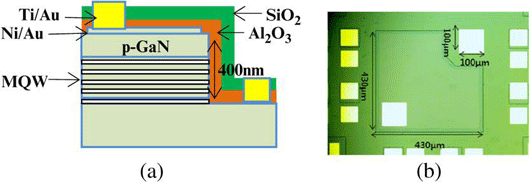
Figure 1: (a) Schematic of the LED configuration. (b) Fabrication of the 430μm x 430μm real LED chip.
The fabrication was then completed by depositing the double dielectric of 5nm aluminum oxide
(Al2O3) by plasma-enhanced atomic layer deposition (ALD) and 50nm silicon dioxide (SiO2) by plasma-enhanced CVD. A Fresnel analysis suggested that the optimum layer thicknesses to maximize the output power would have an Al2O3 layer of 20nm followed by 50nm SiO2. However, such a double-layer would suffer from undesirable reverse current effects that increase as the passivation thickness increases. At normal incidence, it is estimated through a Fresnel analysis that the 50nm/5nm SiO2/Al2O3 structure should allow 10% more light to be transmitted compared with a device without dielectric.
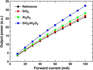 Various passivation layer combinations were tested for LED output power (Figure 2). The double dielectric layer results in about 25% higher output power compared with the unpassivated LED. The dielectric double layer device benefits from improved light extraction through the index of refraction of the SiO2 layer widening the angles at which light can emerge from the device, along with improved electrical performance from reduction of competing non-radiative surface recombination of electrons and holes due to the Al2O3 passivation.
Figure 2: Output power characteristics of unpassivated, SiO2-passivated, Al2O3-passivated, and Al2O3/SiO2-passivated LEDs. The output power of the Al2O3/SiO2-passivated LED is about 25% higher than that of the unpassivated LED.
Parallel conduction through unpassivated surfaces lowers the apparent turn-on voltage of devices. The voltages at 20mA forward current were 3.31V, 3.33V, 3.39V and 3.99V for the unpassivated, the Al2O3-passivated, the SiO2-passivated, and the SiO2/Al2O3-passivated LEDs, respectively.
Al2O3 passivation also reduced reverse leakage current at -5V by two or three orders of magnitude from -1.9x10⁻⁸A (unpassivated) and -7.14x10⁻⁹A (SiO2 passivated) to -3.46x10⁻¹¹A (Al2O3).
Another positive effect is reduced trap state densities estimated at 2.6x10¹¹/eV-cm2 for the Al2O3 passivated device, compared with 6.2x10¹²/eV-cm2 for the SiO2/GaN interface. The lower trap density decreases the amount of competing non-radiative recombination.
The author Mike Cooke is a freelance technology journalist who has worked in the semiconductor and advanced technology sectors since 1997.